Members can download this article in PDF format.
What you'll learn:
- What is a transfer function?
- How to implement a Laplace transform in LTspice.
- Analyzing transfer functions in the frequency and time domains.
- Looking at compensator design in LTspice.
Transfer functions are used in the design of electronic systems such as filters, power supplies, and other control systems. Frequency-domain analysis of a transfer function involves the Laplace transform. This article explores the implementation of a transfer function in LTspice, compares the ideal response to a modeled implementation, and provides several useful examples along the way. Files are available to aid in the understanding and implementation of this topic.
Transfer functions are used when we want to analyze how the output of a system changes depending on the input. The system could be the output voltage of a resistor divider or the speed of a car when you step on the gas. To analyze a system, we want to know how its output amplitude and phase compare with the input over frequency. To do this we use the Laplace transform:
Many resources are available that discuss both the mathematics and intuition of the Laplace transform. For our purposes, we can think of it as a mathematical tool that allows us to work with the gain, frequency, phase, and exponential response of a system.
The basic idea of a transfer function diagram is shown in Figure 1.
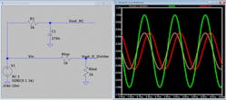
Figure 2 shows two different transfer functions.
The resistor divider is simply described as:
But the RC circuit is described by the slightly more complex Equation 2:
Writing the transfer function in this form allows us to talk in terms of poles and zeros. Here we have a single pole at ωp = 1/RC. While the 1-kHz output of the RC circuit (red trace) is the same amplitude as the resistor divider, the phase delay is notable. The Laplace transform allows us to describe how the RC circuit changes both gain and phase over frequency. The example file is Simple_RC_vs_R_Divider.asc.1
Laplace Transform Syntax in LTspice
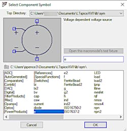
To implement the Laplace transform in LTspice, first place a voltage-dependent voltage source in your schematic. The dialog box for this is depicted in Figure 3.
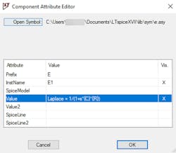
Right click the voltage source element to open its Component Attribute Editor. In the Value field, enter “Laplace = ” followed by your equation, which should contain the complex variable “s.”
In Figure 4, {C} and {R} are placed in curly brackets so that we can use the “.step” Spice command to cycle through some values.
The Figure 5 simulation shows the step response of an RC impedance divider, and the equivalent transfer function written using the Laplace transform. Running the simulation,2 we see that the two outputs match.
As the transfer functions become larger, I have found it useful to use a code editor, which automatically highlights matching parenthesis. Type the equation in the text editor, and then copy it into the LTspice dialog box (Fig. 6).
A Refresher on Poles and Zeros
An example transfer function is given in Equation 3:
Dissecting Equation 3, we first see the term ωp0/s, which is referred to as an origin pole. An origin pole is synonymous with an integrator and is used to provide extremely high gain at low frequencies, thus eliminating steady-state error in a control system. Origin poles result in a constant phase delay of 90 deg. and a gain response of –20 dB per decade. The ωp0 term refers to the frequency at which the gain, due to the origin pole, has rolled off to 0 dB.
Finding the roots of the numerator and denominator gives us the zero and pole frequencies, respectively. Note that the pole/zero frequencies are given by the magnitude (i.e., absolute value) of these roots. A zero results in a phase boost of 90 deg. and an increase of gain around its frequency. A pole results in a phase delay of 90 deg. and a decrease in gain around its frequency.
If instead the example transfer function were written as:
the leading “s” term is now referred to as a zero at the origin. A zero at the origin is representative of a pure differentiator. It has a constant phase boost of 90 deg. and its gain increases with frequency, reaching 0 dB gain at frequency ωz0.
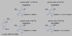
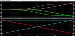
Figure 7 illustrates an example with these various poles and zeros implemented separately. Each has a frequency of 1 kHz. The resulting gain and phase of each is shown in Figure 8. The example file is PoleZeroExamples.asc.3
Comparing the Ideal to Modeled Implementation
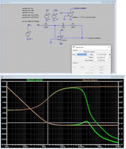
By using LTspice to model a transfer function, you can take advantage of the vast library of modeled components. As a first example, let’s look at an inverting op amp providing proportional gain. Ideally H(s) = –Rp/Ri. This should result in a simple scaling of the input voltage and a phase shift of 180 deg. But as illustrated in Figure 9, at about 320 kHz, the gain has rolled off from the ideal by 3 dB and the phase shifted significantly. This follows from the gain bandwidth of the LT6015 being 3.2 MHz, and the circuit in Figure 9 having a gain of –10 V/V.
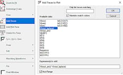
In LTspice, it’s possible to enter your own equations into the waveform viewer. If we want to see the gain and phase difference between our ideal equation and the op-amp-based circuit, then we add a new waveform. This is done by right clicking on the waveform viewer and selecting Add Traces. The expression can then be added to the plot one node divided by the other (i.e., V(vout_pro)/V(vout_laplace)) (Fig. 10).
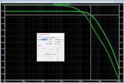
The gain and phase comparison are shown in Figure 11, which makes it easy to see that, at low frequencies, we have 0 dB in gain difference and no discrepancy in phase. The example file is ProportionalGain.asc.4
Second-Order RLC System
The general form of a second-order system is given by the Simon Bramble article, “Electronic Control Theory of Second-Order Systems: A Practical Analysis for Engineers.”5
When implemented as an LRC, we have:
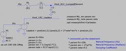
The LTspice implementation is shown in Figure 12. The example allows you to specify R, L, and C, or alternatively you can specify the damping factor ζ and resonant frequency ωn.
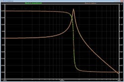
Figure 13 reveals the frequency response of this second-order system. The peaking shown is often undesirable, requiring damping when designing something like an input EMI filter for a buck regulator. The example file is LRC_AC_Analysis.asc.6
Differentiator and the Safety Pole
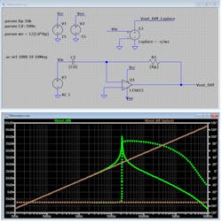
A differentiator is shown in Figure 14.
As expected, the origin zero results in a 20 dB/decade increase in gain over frequency. Differentiators are utilized to increase response to high-frequency signals. In practice, pure differentiators aren’t used and instead are implemented with the addition of a safety pole. A safety pole is placed so that a system isn’t overly sensitive to high-frequency noise. Also, notice the resonant peak shown in the op-amp implementation. This peak may prove problematic when attempting to control a system.
The implementation in Figure 14 has the zero (where gain crosses 0 dB) at:
In our example, a safety pole is implemented at five times this value. Figure 15 shows a differentiator plus safety-pole implementation. The pole frequency we desire is at 5 × 159 Hz = 796 Hz. To achieve this, we place a feedback capacitor with one-fifth the value of the input capacitor. The full transfer function is given by:
where ωz = 1/RpCd and ωp = 1/RpCi . The simulation (Fig. 11, again) shows us that this safety pole reduces both the gain and phase as the pole frequency is approached. The peaking due to the op amp also is reduced.
First-Order Plus Delay (FOPD)
When modeling the behavior of a system, the FOPD model is a useful tool. For a more complete explanation, read Dr. John D. Hedengren’s “Dynamic Process Modeling” lecture.7 In short, a process can be described by a fixed delay, a full-scale response, and a time constant. To implement a fixed delay, we take advantage of the following Laplace transform:
As a reminder, a time constant is defined by 1 –1/e = 63.2%. The FOPD model comes out as:
where:
kp = full-scale output
𝜏F = time constant
𝛳F = time delay
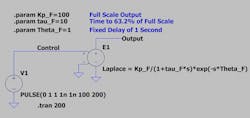
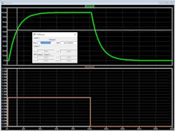
Figure 16 shows the implementation of a system having a full scale of 100, a time constant of 10 s, and a delay of 1 s. Because the input step is applied at t = 1 s, it follows in Figure 17 that at t = 12 s, the output is at 63.2 V. The simulation file is FOPD.asc. 8
Compensator Design in LTspice
Control system design is a rich field that spans many disciplines. A key component to a closed-loop control system is the compensator. Once the transfer function of system to be controlled is known, the compensator is designed to address the gain and phase adjustment needed for closed-loop stability and performance.
PI (Type 2a) Compensator
Many systems can be compensated with a Type 2a compensator, which consists of a pole at the origin (integrator) plus a zero. Negative feedback provides 180 deg. of phase delay, while the pole at the origin results in another fixed 90 deg. of delay. By placing a zero, that additional 90 deg. phase shift is removed at higher frequencies. With this approach, we can decide how much phase shift we want at a specific frequency and place the zero accordingly.
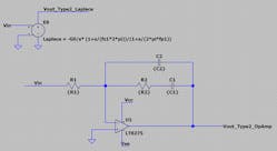
An op-amp-based Type 2a controller is shown in Figure 18.
The Type 2a transfer function is written as:
The origin pole frequency is given by ωp = 1/R2Ci and the zero frequency is ωz = 1/R2Ci.
The effect of the op amp here is again apparent, with both gain and phase rolling off from the ideal at higher frequencies. The example file is Type2a.asc.9
Type 2 Compensator
The Type 2 compensator consists of an origin pole plus a pole/zero pair and takes the form shown in Figure 19.
The transfer function is given by:
With pole/zero locations of:
At this point, the designer faces a dilemma. The choice of Rs and Cs affects both the pole and zero. Also, the question of where to place the pole and zero needs to be addressed. The book Designing Control Loops for Linear and Switching Power Supplies derives and gives an example of how to step through the design process.
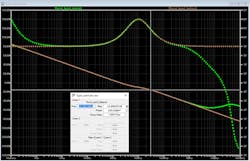
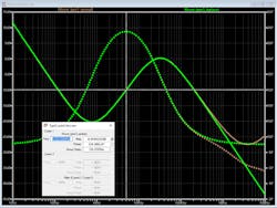
To aid the reader, this method is applied and given in the LTspice example file, Type2_autoCalcs.asc.10 The output of this example is shown in Figure 20. The goal of 10-dB attenuation with a 30-deg. phase boost at 10 kHz is achieved. Once again, the nonideal properties of the op amp show up at higher frequencies.
Type 3 Compensator
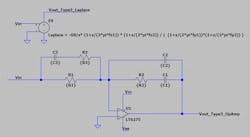
A Type 3 compensator takes the form shown in Figure 21.
The motivation for this more complex transfer function is that we can get access to a larger phase boost. Negative feedback gives us the initial 180 deg. of delay. But now we have access to two zeros with the potential of boosting phase by 180 deg. Two poles are placed to roll off the high-frequency gain and phase. The transfer function is given by:
with pole/zero locations of:
As with the Type 2a compensator, the process of choosing pole/zero locations and then calculating the Rs and Cs is involved. The book Designing Control Loops for Linear and Switching Power Supplies derives and gives an example of how to step through the design process.
To aid the reader, this method is applied and given in the LTspice example file Type3_autoCalcs.asc.11 The output of this example is illustrated in Figure 22. The goal of 10-dB attenuation with a 145-deg. phase boost at 5 kHz is achieved. Once again, the nonideal properties of the op amp show up at higher frequencies.
Origin Pole in the Time Domain
Up to this point, we’ve shown how LTspice can implement a transfer function by using circuit elements and the Laplace transform. Examples shown have been in the frequency domain. It may naturally follow to analyze these transfer functions in the time domain (i.e., a step response).
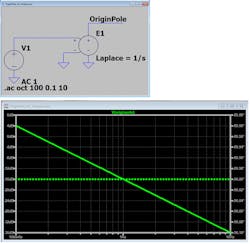
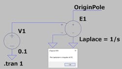
To do this, we need to address the issue of the origin pole and how to implement it. A transfer function with an origin pole (i.e., pure integrator) is H(s) = 1/s. This transfer function works fine in the frequency domain (Fig. 23), but in the time domain we get an error (Fig. 24).
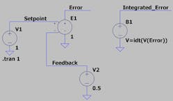
To get past this issue, we can instead use the behavioral voltage source and the idt() function (Fig. 25). Figure 25 also gives the beginnings of a feedback system, which compares a setback to a static feedback voltage. The example file is OriginPole_TransientAnalysis_idt.asc.12
Filter Design
The Linear Circuit Design Handbook13 is part of Analog Devices’ extensive library of educational materials. Chapter 8 discusses analog filters. The Laplace representation of the filters discussed in this chapter are given as an example file, Laplace_Filters_LinearSystemsBook.asc.14 Please refer to the filter design section of the Precision Toolbox, which aids in the design of active filters.15
Conclusion
Numerous examples have been given of how to implement a transfer function by comparing the lumped-element representation to a Laplace-transform-based equation. These examples are educational, in the sense of connecting classroom theory to circuit implementation, and they aid in the practical design of various compensators. It’s important to note that, for switch-mode power supplies, LTpowerCAD is a powerful (and preferred) resource for compensation design.16 While LTspice may be used to work with and understand some compensators, in the case of power-supply design, LTPowerCAD is more well-suited.
Acknowledgements
Simulations were conducted in LTspice. Thank you to Dr. Shalom D. Ruben, University of Colorado Boulder, for his guidance on this article.
References
1. Simple_RC_vs_R_Divider.asc. Analog Devices, Inc.
2. Laplace_Simple_RC.asc. Analog Devices, Inc.
3. PoleZeroExamples.asc. Analog Devices, Inc.
4. ProportionalGain.asc. Analog Devices, Inc.
5. Simon Bramble. “Electronic Control Theory of Second-Order Systems: A Practical Analysis for Engineers.” Analog Dialogue, Vol. 54, No. 3, September 2020.
6. LRC_AC_Analysis.asc. Analog Devices, Inc.
7. John D. Hedengren. “Dynamic Process Modeling.”
8. FOPD.asc. Analog Devices, Inc.
9. Type2a.asc. Analog Devices, Inc.
10. Type2_autoCalcs.asc. Analog Devices, Inc.
11. Type3_autoCalcs.asc. Analog Devices, Inc.
12. OriginPole_TransientAnalysis_idt.asc. Analog Devices, Inc.
13. Linear Circuit Design Handbook. Analog Devices, Inc., 2008.
14. Laplace_Filters_LinearSystemsBook.asc. Analog Devices, Inc.
15. ADI Precision Studio. Analog Devices, Inc.
16. Henry Zhang. “Application Note 149: Modeling and Loop Compensation Design of Switching Mode Power Supplies.” Linear Technology, January 2015.
Basso, Christophe. Designing Control Loops for Linear and Switching Power Supplies. Artech House, October 2012.
Differentiator_SafetyPole.asc. Analog Devices, Inc.
Type3_autoCalcs_steps.asc. Analog Devices, Inc.
