How to Design Very Wide Loop BW High-Performance PLL Frequency Synthesizers (Part 2)
What you’ll learn:
- A special technique to produce very wide loop BWs in high-frequency PLLs (and hence, indirect (PLL) synthesizers), thereby achieving very low phase noise rivaling that of direct (MMD) synthesizers.
- A modified standard PLL design procedure for a Type 2 - 2nd Order system with a 1st Order active proportional-integral (PI) loop filter, which uses the special technique.
- A method of modeling and simulating complex PLL topologies using the high degree of flexibility of a general frequency-domain simulator, rather than using the limited degree of flexibility of a specific PLL simulator, which is meant for simple PLL topologies.
This is Part 2 of a three-part series.
As discussed in Part 1 and recapped here, modern wireless communications systems (mainly superheterodyne radio transceivers) are now required to deliver higher performance than ever before, and they’re placing greater demands on the frequency sources for these systems. Such systems are moving higher in frequency (millimeter-wave, or mmWave, and possibly THz regions), tuning wider bandwidths (BWs), processing more complex waveforms using more elaborate modulation schemes, and operating in fast tuning modes.
This is happening in both the commercial and military arenas. Examples include satellite communications and repeaters, terrestrial wireless systems such as the present 5G15,16 and eventually 6G17,18 protocols, and tactical line-of-sight radios, among others. Therefore, the frequency sources, and particularly the local oscillators (LOs), for these systems must also move commensurately higher in frequency and deliver higher performance in terms of low phase noise (our priority interest), low spurious, and fast tuning speed.
In some cases, LOs using direct (mix-multiply-divide, MMD) synthesizers are needed to achieve this performance, but they’re usually not lowest in SWaP, cost and complexity. However, in many cases, LOs using indirect (phase-locked-loop, PLL) synthesizers can be used with excellent results. They rival the performance of direct synthesizers and are usually lowest in SWaP, cost, and complexity, which is the thesis here.
For the case of PLL synthesizers and, concerning a priority interest in low phase noise, this means that for the relevant PLLs, as their operating frequencies become higher, their loop BWs must become commensurately wider (i.e., fractional loop BW is the ultimate interest) to achieve low phase noise. Also, by applying the special technique shown here, it’s possible to achieve very wide loop BWs in such synthesizers, which can’t be achieved by conventional methods.
By “relevant PLLs,” we mean those PLLs comprising the synthesizer that significantly influence the operating band phase noise. For multiple PLL systems, this usually means the output PLL, which is normally the highest frequency PLL. For single PLL systems, the situation is obvious.
In addition to utilizing very wide loop BWs, the use of unity closed-loop (CL) gain along with only internal (within any relevant PLL) multiplication also assists in achieving low phase noise. The technique is applied here to an example synthesizer that’s a single-loop (thereby having only one relevant PLL, simplifying the situation), Type 2 - 2nd Order system with a 1st Order active proportional-integral (PI) loop filter, which is used as an LO in an actual working and fielded high-performance receiver.
This topology is widely employed, so the technique has broad applicability. It can also be applied to PLLs using other topologies with appropriate modifications. However, we will restrict our discussion to the topology of our example mentioned above. Also, the example synthesizer is based on analog hardware because of the high-frequency loop dynamics involved, rather than digital (or computed) hardware/software approaches, which are limited by present-day computing speeds.
In Part 1 we described the technique and presented the example synthesizer incorporating the technique. In Part 2, we discuss the synthesizer general design approach and detailed design, which incorporates the technique.
>>Check out Parts 1 and 3 of this series

General Design Approach and Block Diagram
Initially, complete system (receiver) and subsystem (1st LO) analyses were done, with priority interest in low phase noise, followed by a trade study to decide on the general design approach for the synthesizer, i.e., either direct (MMD) or indirect (PLL), along with the number of MMDs or PLLs (loops) needed, respectively. The indirect (PLL) approach was decided upon, for the following reasoning:
- The direct approach typically has lower phase noise and faster switching speed (although spurious can be somewhat more troublesome) than with the indirect approach, but has higher SWaP, cost and complexity. This approach wasn’t chosen based mainly on the latter issue.
- The indirect approach typically has higher phase noise and slower switching speed (although spurious can be somewhat less troublesome) than with the direct approach, but has lower SWaP, cost and complexity. This approach was chosen based mainly on the latter issue.
Then, continuing with the analyses and reasoning above, along with the specifications described in the “Example Synthesizer Application and Specifications” in Part 1, it was decided on the following detailed implementation for our PLL approach:
- Topology:
- Single loop (only one PLL deemed necessary)
- Type 2 - 2nd Order system with a 1st Order active PI loop filter
- Translational feedback (FB) - providing unity (N = 1 or 0 dB) CL gain
- Internal (within PLL) multiplication
- Acquisition: Aided (necessitated by its wide tuning BW and unity CL gain), using window steering circuit
- Loop BW, fG (= ωG / 2π), chosen for lowest integrated SSB phase noise: fG = 15 MHz
- Natural resonant freq, fn (= ωn / 2π), and damping factor, ζ (recall fG = 15 MHz):
- fn = 9.677 MHz (using rule-of-thumb fn = fG / 1.55 for ζ = 0.7072), ζ = 0.707
- 1st Order active PI loop filter (detail): Dual-path topology, i.e., a 1st Order dual-path active PI loop filter, since a single-path topology (normally an op amp) would not support the very wide loop BW
- Translational FB (detail): Dual conversion (two sequential converters)
So, in summarizing, it was concluded that the synthesizer would be of the PLL variety with the following topology: Single Loop, Type 2 - 2nd Order system with a 1st Order dual-path active PI loop filter, dual conversion translational FB, internal multiplication, aided acquisition, loop BW of 15 MHz, natural resonant frequency of 9.677 MHz, and damping factor of 0.707. For discussion purposes, the synthesizer will be broken up into two sections: the “PLL Section” and the “Reference - I/O - Power Section.
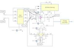
PLL Section
Figure 1 shows the block diagram of the PLL Section.
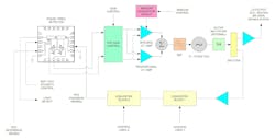
This section begins with the phase frequency detector (PFD), which has a 1,300-MHz BW, up and down (i.e., two) voltage outputs (each output being differential, for a total of four voltage outputs), a very low SSB phase-noise floor factor of −153 dBm/Hz, no dead zone, internal polarity control, and lock detection capability. It feeds a gain control circuit providing approximately 0 to −7.5 dB of adjustment in 16 steps of 0.5 dB, which then feeds the 1st Order dual-path active PI loop filter.
The loop filter contains a low-noise op-amp integral (integrating) amplifier in parallel with a discrete, low-noise, differential proportional amplifier, along with an aided acquisition (window steering) circuit. The output of this system, after being summed and filtered, then controls a 5- to 10-GHz wideband VCO that feeds an effective X4 internal multiplier for the 22.5- to 39.9-GHz synthesizer output. Finally, we have the dual conversion translational FB system completing the loop.
These three design techniques provide unity CL gain and very low phase noise. Better phase noise might be possible using a switched, narrowband VCO stack. However, a single wideband VCO was used for lower SWaP, cost, and complexity, while providing phase noise that met subsystem (and hence, system) specifications with reasonable margin.
Reference - I/O - Power Section
Figure 2 shows a simplified block diagram of the Reference - I/O - Power Section.
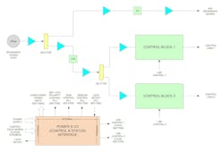
This section begins with a state-of-the-art 100-MHz OCXO that goes through a 2X splitter. One output of the splitter drives an effective X4 multiplier to provide the 400-MHz PFD reference to the PLL section and the other output drives an effective X16 multiplier that goes through another 2X splitter.
Both outputs of that splitter drive two control blocks, Control Block 1 and Control Block 2, where each of these produces its respective control lines, Control Lines 1 and Control Lines 2. The lines drive their respective converter blocks, Converter Block 1 and Converter Block 2, in the PLL Section.
Finally, we have the Power & I/O (Control & Status) Interface, which is fairly typical, showing those functions that interact internal to the synthesizer and those that interact external to the synthesizer. Also labeled are those functions that interface with the local section (Reference - I/O - Power Section), PLL Section, and both sections.
The 1st Order dual-path active PI loop filter is the key component of the synthesizer that allows it to achieve its very wide 15-MHz loop BW (Fig. 3).
The op-amp integral amplifier is standard and not a contributor to the very wide loop BW. However, the differential proportional amplifier is unique, and it’s the sole contributor to the very wide loop BW (Fig. 3 and close-up in Fig. 4). This is because of its high frequency operation; for the example design, at a bias point of 3 V – 3 mA, the insertion gain of each device is 15 dB at 300 MHz with a transition frequency (fT) of 2 GHz (as indicated by the S-parameter data from the device datasheet).
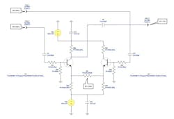
It also provides a great deal of flexibility, since its gain (and other parameters) can be adjusted. With the adjustable gain, wider loop BWs can be achieved (to perhaps 100 MHz or more, if ever practically needed) if not limited by the VCO tuning port modulation BW. As good design practice, each input to the amplifier is fed by a 50-Ω source impedance from each output of the PFD, which varies slightly with PFD gain control setting. The amplifier output is then terminated with a 50-Ω load impedance at the summing point with the op-amp integral amplifier.
PLL Section Detailed Design and Schematic Diagram
The design of any PLL and, hence, our single-loop PLL synthesizer, can basically be systemized into a straight-forward sequence of standard steps.2 Except for the special loop filter, the detailed design of the loop is a fairly straightforward textbook example for a Type 2 - 2nd Order system with a 1st Order active PI loop filter. Some of these design steps were already determined in the “General Design Approach and Block Diagram” section above, and they’re repeated here for comprehensiveness and with further clarification. These design steps are:
1. Interpret and understand specifications:
- As discussed in the “Example Synthesizer Application and Specifications” section in Part 1.
2. Select general approach and implementation:
- As discussed in the “General Design Approach and Block Diagram” section above.
3. Select components (ones with major impact to performance - all are low-noise/low-power types): Reference oscillator (actually in Reference - I/O - Power Section), VCO (Ko = Kv/s), PFD (Kϕ), FB divider (Kn = 1/N), Loop filter / Error amplifier (F(s) - comprised of individual proportional and integral error amplifiers):
- Reference oscillator: Major electronics manufacturer’s state-of-the-art 100-MHz OCXO.
- VCO: Major electronics manufacturer’s high-frequency octave BW (5-10 GHz) VCO, along with X4 internal (within PLL) multiplier, to produce effective:
- Kv = 875 MHz/V => 5.498(109) rad/S/V @ 39.9 GHz (upper band edge)
- Kv = 1,355 MHz/V => 8.514(109) rad/S/V @ 31.3 GHz (middle of band)
- Kv = 1,635 MHz/V => 1.027(1010) rad/S/V @ 22.5 GHz (lower band edge)
- PFD: Major electronics manufacturer’s wideband (1,300 MHz) low-noise (−153 dBm/Hz SSB phase-noise floor factor) PFD, along with gain control, to compensate for Kv variations across the VCO band (keeping KϕKv = constant) to produce effective:
- Kϕ = 5.556 mV/deg => 0.318 V/rad @ 39.9 GHz (upper band edge - gain at maximum)
- Kϕ = 3.582 mV/deg => 0.205 V/rad @ 31.3 GHz (middle of band - gain at mid-range)
- Kϕ = 2.970 mV/deg => 0.170 V/rad @ 22.5 GHz (lower band edge - gain at minimum)
- FB divider: None - dual conversion translational FB used, giving N = 1, Kn = 1/N = 1.
- Proportional error amplifier: Major electronics manufacturer’s bipolar differential pair (low-noise, low-power, high-frequency, compatible power-supply requirements, adequate output voltage/current drive capabilities).
- Integral error amplifier: Major electronics manufacturer’s high-performance op amp (low-noise, low-power, unconditional stability, compatible power-supply requirements, adequate output voltage/current drive capabilities).
4. Determine PLL topology:
- Since phase continuity for adjacent channel step phase and frequency is specified, a Type 2 PLL is required. A 2nd Order (excluding any extra high-frequency poles used for additional filtering) PLL will be used because it’s (theoretically) unconditionally stable, is the minimum order that can be used, and is less complex than higher-order systems. Also, a 1st Order dual-path active PI loop filter will be used since a standard active PI loop filter (normally a single op amp) will not support the very wide loop BW. These three factors make the PLL simple, easily analyzed, and unconditionally stable. In summary, then, the PLL will be a Type 2 - 2nd Order system with a 1st Order dual-path active PI loop filter. The special loop filter will be implemented by using a standard op amp for the integral part and a differential amplifier for the proportional part.
- As shown in Figures 3 and 4, the differential amplifier in this case isn’t a true differential amplifier, but rather a pseudo-differential amplifier. We use the prefix “pseudo-” because it doesn’t have the two emitters coupled together biased with a true current source. Rather, it has each emitter independently biased with a relatively high-value “long tail” resistor, approximating a true current source, and a low-value cross-coupling resistor between the two emitters, which partially controls the gain. This circuit is a standard substitute for a true differential amplifier because of its simplicity and it works well for this application.11 The bias point for each device (both devices in a single package) was chosen from the datasheet at 3 V – 3 mA based on S-parameter data for these conditions. Then the gain of the amplifier using our implementation is given by G = (R3/2R2).
5. Determine standard parameters ωn and ζ from the specifications:
- ωn (actually fn) and ζ are determined from phase noise, switching time, and stability specifications. For this case, phase noise is the priority. These were determined in the “General Design Approach and Block Diagram” section above to be (recall fG = 15 MHz):
fn = 9.677 MHz (using rule-of-thumb fn = fG / 1.55 for ζ = 0.7072)
ζ = 0.707
6. Equate the standard-form OL transfer function to the circuit-constant OL transfer function, which gives standard parameters fn and ζ as functions of circuit constants R1, R2, R3, and C1 (recall ωn = 2πfn):
G(s)H(s) = 2ζωn/s + ωn2/s2 (standard-form)
= KϕF(s)KoKn (circuit-constant)
= KϕF(s)Kv/sN
= {Kϕ[(sτ2 + 1)/sτ1]Kv}/sN
= [(KϕKvτ2)/(Nτ1)]/s + [(KϕKv)/(Nτ1)]/s2
where:
- F(s) = (sτ2 + 1)/sτ1
- τ1 = R1C1
- τ2 = R3R1C1/2R2
which we plug into the circuit-constant OL transfer function to obtain the desired relations:
ωn = (KϕKv/Nτ1)0.5 = (KϕKv/NR1C1)0.5
ζ = (τ2/2)(KϕKv/Nτ1)0.5
= (R3R1/4R2)(KϕKvC1/NR1)0.5
= ωnτ2/2
= ωnR3R1C1/4R2
7. Solve for (calculate) initial values of circuit constants R1, R2, R3, and C1 as functions of standard parameters wn and z, and calculate any other quantities of interest:
τ1 = KϕKv/ωn2N
τ2 = 2ζ/ωn = 2ζ(Nτ1/KϕKv)0.5
R1 = KϕKv/ωn2NC1
R2 = ωnR3R1C1/4ζ = (R3/4ζ)(KϕKvR1C1/N)0.5
C1 = KϕKv/ωn2NR1
Note that R1, R2, R3, and C1 aren’t uniquely determined, so an absolute selection must be made for two of these values, usually C1 and R3. Select C1 and R3, then calculate R1 and R2:
C1 = 200 pF, R3 = 51 Ω, R1 = 513.5 Ω (std 5% value 510 Ω), R2 = 112.6 Ω (std 5% value 110 Ω).
8. Model PLL and simulate performance using a general frequency-domain modeling/simulation tool:
- Genesys, from Keysight Technologies - PathWave Design Division, was used in this case. Adjust OL gain and initial circuit values in model as needed for proper loop dynamics performance from simulations - due to unavoidable discrepancies that usually arise between initial circuit values and adjusted circuit values in model.
9. Build and test EDM unit:
- Using model adjusted circuit values, build and test the EDM unit. Adjust EDM circuit values as needed for proper loop dynamics performance from EDM, due to unavoidable discrepancies that usually will arise between simulated performance and actual EDM performance. The final EDM adjusted circuit values turned out to be:
C1 = 510 pF, R3 = 51 Ω (unchanged - proportional amplifier load), R1 = 1,000 Ω, R2 = 220 Ω
10. Adjust model OL gain as needed for agreement between model and EDM unit:
- This is best done by adjusting the value of R4 in parallel with the PFD gain control (Fig. 3. again).
These were the design steps used for the PLL and, hence, our single-loop PLL synthesizer. Also shown in Figure 3 are the PFD (voltage output) gain control block, the 1st Order dual-path active PI loop filter circuit, the PFD reference / sub-harmonic filter block, and the aided acquisition (window steering) block.
The PFD gain control is included to compensate for the variation in effective Kv of 5.4 dB (20 Log (1,635 MHz / 875 MHz)) across the operating band. It consists of a switched resistive voltage divider across the PFD up/down outputs providing approximately 0 to −7.5 dB of adjustment in 16 steps of 0.5 dB. The 1st Order dual-path active PI loop filter has a transfer function zero or transition point of 300 kHz, which is where the transition from the integral (op amp) amplifier to the proportional (differential) amplifier occurs.
The PFD reference / sub-harmonic filter is an LC band-stop type and consists of a 100-MHz full transform band-stop, a 200-MHz single-resonator trap, and a 300-MHz single-resonator trap. The 400-MHz reference should be very well filtered by the loop filter. It was found experimentally that this was indeed the case, so no additional filtering was needed for the 400 MHz reference.
The X4 internal multiplier actually consists of two X2 multipliers because the VCO has its signal path split into two separate signal paths after the first X2 multiplier, each maintaining equal fractional BWs, to be able to properly filter the VCO harmonic spurious. The aided acquisition (window steering) circuit confines the VCO to remain within the operating BW of the PFD and the lock-in range of the PLL.
The above information will be used in the upcoming Part 3, where we model and simulate the example synthesizer PLL section loop dynamics and measure its critical characteristics, which demonstrates the excellent performance achieved using the technique.
Acknowledgements
This paper represents the coalescence, organization, and technical writing by the author of the work done by a number of top technical professionals with expertise in frequency synthesizers, radio/radar, and communications systems. It especially represents the work done by Ben Nardi staff scientist and subject-matter expert in these areas who initiated the synthesizer concept and original design, and who produced a prototype unit.
It was a pleasure for the author to have worked with and to have exchanged ideas with these professionals and, particularly, Mr. Nardi. It allowed the author to assume leadership of the synthesizer with his own team, thereby adding his own ideas and developing it to its final production condition. This gave the author the ability to write this paper and, in doing so, further solidified and expanded his knowledge of the subject of PLLs and indirect (PLL) synthesizers.
References
1. F.M. Gardner, Phaselock Techniques, 3rd ed., Wiley, Hoboken, NJ, 2005
2. R. E. Best, Phase-Locked Loops, Design, Simulation and Applications, 6th ed., McGraw-Hill, New York, 2007
3. P. V. Brennan, Phase-Locked Loops: Principles and Practice, McGraw-Hill, New York, 1996.
4. E. Drucker, “Phase Lock Loops and Frequency Synthesis for Wireless Engineers,” 1997, Frequency Synthesis & Phase-Locked Loop Design, three-day short course, Besser Associates, Mountain View, CA, 1999.
5. B. Nardi, personal communication, Gaithersburg, MD, 2008.
6. A. Harney, “Designing High-Performance Phase-Locked Loops with High-Voltage VCOs,” Analog Dialogue 43-12, Analog Devices, December 2009.
7. R. C. Dorf and R. H. Bishop, Modern Control Systems, 9th ed., Prentice-Hall, Upper Saddle River, NJ, 2001.
8. W. J. Palm, III, Modeling, Analysis, and Control of Dynamic Systems, 2nd ed., Wiley, New York, 2000.
9. G. Ellis, Control System Design Guide, 2nd ed., Academic Press, San Diego, 2000.
10. W. H. Hayward, Introduction to Radio Frequency Design, Prentice-Hall, Englewood Cliffs, NJ, 1982.
11. S. A. Sedra and K. C. Smith, Microelectronic Circuits, 6th ed., Oxford University Press, New York, 2010.
12. “Control System Development Using Dynamic Signal Analyzers,” Application Note 243-2, Hewlett-Packard Co., Palo Alto, CA, 1984.
13. Motorola Communications Device Data, Data Book, DL136/D, REV 4, Phoenix, AZ, 1995.
14. F. C. Weist, “Phase Locked Loop Basics for Frequency Synthesizer Applications,” 2010, short course presentation (© 2010 by Frederick Weist), Clarksburg, MD, 2010.
15. “What Frequency Bands Will Roll Out the Carpet for an Official 5G Standard?,” Microwaves & RF magazine, Vol. 56, No. 6, June 2017, p. 20.
16. “Navigating the 5G NR Standards,” Microwave Journal, Vol. 61, No. 12, December 2018, p. 72.
17. S. Pongratz, “6G and The Long RF Journey Ahead,” Microwave Journal, ePublishing Online Article, February 2024.
18. C.-X. Wang et al., “On the Road to 6G: Visions, Requirements, Key Technologies and Testbeds,” IEEE Communications Surveys & Tutorials, Vol. 25, No. 2, Second Quarter 2023, pp. 905 – 974.
>>Check out Parts 1 and 3 of this series
About the Author

Frederick Weist
Principal, FCW Sciences
Frederick Weist presently resides in Point Of Rocks, Md. He was born in Philadelphia, Pa., on March 25, 1959. He obtained his BS in physics from Drexel University, Philadelphia, in 1983 and his MS in physics from the same institution in 1992.
He is presently (semi-) retired, but continues his interest in STEM research, writing and publishing by working as Owner, FCW Sciences, Point Of Rocks, Md. His last position was as Principal Engineer / SME with Boeing Co. - Digital Receiver Technology Subsidiary, Germantown, Md. Previously he held positions as Consultant with Planar Monolithics Industries (PMI), Senior Design Engineer with Kratos Defense and Security Solutions - Herley-CTI Division, Principal Engineer with DRS Technologies - Signal Solutions Division, Senior Engineer with Aydin Corp. - Telemetry Division and Electronics Engineer with the U.S. Naval Air Warfare Center - Aircraft Division (NAWCAD).
His previous interests included research, design, and development of systems from DC to 42 GHz, specializing in PLLs, frequency synthesizers, transceivers, subsystems, and components. He has also worked in the fields of servos, sonar, photonics, magnetics, and superconductivity. His present interests include the same as well as integrated microwave / photonics (IMWP), quantum, and biophysics systems.
He is a member of the American Physical Society and the Institute of Electrical and Electronics Engineers.
Comment About the Article
To join the conversation, and become an exclusive member of Electronic Design, create an account today!

Leaders relevant to this article: