What’s the Difference Between Continuous-Time and Discrete-Time Sigma-Delta ADCs?

Sigma-delta analog-to-digital converters (ADCs) can effortlessly achieve an effective number of bits (ENOB) of 24 bits or higher, making them exceptionally suitable for the precision measurement of micro-signals. These converters are widely utilized in applications such as electronic scales, pressure gauges, industrial temperature sensors (e.g., resistance temperature detectors/thermocouples), high-fidelity audio recording and playback, and physiological signal monitoring (e.g., ECG, EEG).
Compared to successive-approximation-register (SAR) or pipeline ADCs, traditional sigma-delta ADCs trade speed for precision by necessitating oversampling and averaging, which limits the output data rates. However, the advent of continuous-time (CT) sigma-delta ADCs has enabled output rates to escalate from hundreds of samples per second to the mega-sample range, significantly broadening their application scope. This article digs into the architecture of CT sigma-delta ADCs and provides a comparative analysis with discrete-time (DT) variants.
Given that the primary industrial utility of sigma-delta ADCs lies in precision signal acquisition, signal-to-noise ratio (SNR) and ENOB serve as the critical metrics for performance evaluation.
Here, we’ll leverage Analog Devices’ signal chain designer to model common industrial scenarios, including DC voltage, mid-to-high frequency AC voltage, pressure sensors, and current detectors. The AD4134 (CT) and AD7768-1 (DT) are used as benchmarks to observe their respective SNR and ENOB performance.
Basic Architecture of DT Sigma-Delta ADCs
The Modulator
Figure 1 illustrates a complete block diagram of a sigma-delta ADC, where the modulator serves as the core module. In a DT sigma-delta architecture, the analog input signal is first captured by a sample-and-hold (S&H) circuit before entering the modulator loop. The modulator operates at an oversampling clock frequency and updates its output (via the quantizer) at every clock cycle. This process generates a high-speed, low-bit digital bitstream, which serves as the input for the subsequent digital filter and decimation stages.

A simple linear model of a first-order sigma-delta modulator can be used for illustration:
X(z): Input signal
E(z): Quantization noise (assumed to be additive white noise) H(z) = Z−1/1 – Z−1: Integrator (delayed accumulation)
Y(z): Output signal
Based on feedback control theory, the output can be expressed as:
Y(z) = X(z) STF(z) + E(z) NTF(z)
where:
Signal transfer function (STF): STF(Z) = Z−1 (representing a pure delay)
Noise transfer function (NTF): NTF(Z) = 1 – Z−1 (representing a high-pass filter)
When transforming to the frequency domain by setting Z = ejωt, the magnitude of the noise term is: |NTF(f)| = 2/sin(π f/fs). As the frequency approaches zero (near DC or low-frequency signals), |NTF(f)| approaches zero. This demonstrates that the noise is significantly suppressed at low frequency.
>>Download the PDF of this article

From a system-level perspective, the number of zeros in the NTF increases with the order of the modulator, causing more quantization noise to be pushed out of the signal band. This frequency-domain behavior further translates into an improvement in the overall SNR. Taking the first-order sigma-delta modulator as an example, the SNR can be estimated using the following formula:
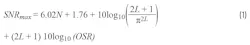
As indicated by the formula, a higher modulator order results in a superior SNR value. In addition, the formula includes the oversampling ratio (OSR).
Oversampling
When an analog input is sampled at a sampling rate FS, the Nyquist frequency is defined as FS/2 within the entire range from DC to FS. The noise is generally distributed uniformly (flat) with a magnitude of 1 LSB. Figure 2a illustrates the characteristics of a typical SAR ADC: When the analog input is sampled, the noise floor remains flat across the bandwidth of interest, from DC to the Nyquist frequency.

Figure 2b demonstrates the effect of sampling the analog input at KFS instead of FS, where the OSR K is typically a factor of 16 or 32. This sampling frequency is significantly higher than the signal bandwidth of interest from DC to FS/2.
Oversampling offers several advantages, most notably the simplification of antialiasing filter (AAF) design. What are the primary benefits of oversampling? First, as shown in Figure 2, since the sampling occurs at KFS, the Nyquist zone extends far beyond the original range. While the total integrated noise power remains constant, it’s now spread across a much wider frequency spectrum. Consequently, the noise spectral density within the baseband (the frequency band of interest) is significantly reduced.
In summary, the primary advantage of oversampling the analog input is the reduction of in-band noise. For every doubling of the OSR, the SNR improves by approximately 9 dB (equivalent to an increase of 1.5 bits in resolution).
Noise Shaping and Decimation
Next is the digital filtering stage, typically implemented as a sinc filter. Observing the noise spectrum once more, since the noise is distributed over a broader bandwidth, the in-band noise is further reduced.
A pivotal feature of sigma-delta converters is noise shaping, which suppresses noise within the band of interest by pushing it toward higher frequencies. This spectral redistribution is illustrated in Figure 2c. Due to this shaping effect, the digital filter can easily attenuate the high-frequency noise components outside the signal bandwidth.
Decimation is based on the concept of signal and noise averaging. By downsampling the output of the digital filter, the signal is further averaged, a process mathematically equivalent to passing the signal through a low-pass filter. Intuitively, decimation enhances signal quality and achieves a lower noise floor.
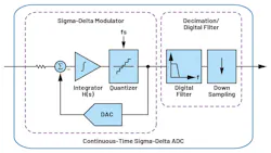
CT Sigma-Delta ADC Architecture
Unlike DT sigma-delta ADCs, which require an S&H circuit to sample the analog input first, CT sigma-delta ADCs eliminate this front-end stage. Instead, the signal enters the modulator directly, and sampling occurs at the quantizer stage (Fig. 3).
In DT architectures, the S&H circuit presents a capacitive input impedance. The internal sampling capacitor must be fully charged within a very short sampling window.
Designing a driver circuit that ensures rapid charging and settles without ringing—to avoid sampling dirty or unsettled signals—is a significant engineering challenge. This typically necessitates high-speed, high-precision operational amplifiers (op amps), which are often costly and increase both the bill-of-materials (BOM) cost and the PCB footprint.
By eliminating the S&H circuit, the input of a CT sigma-delta ADC presents a resistive input impedance (Fig. 4). Driving a resistive load is significantly easier than driving a capacitive one. For signal sources with low output impedance, the signal can often be interfaced directly with the ADC, simplifying the overall signal chain design.

In addition, the CT sigma-delta modulator incorporates integrators, a quantizer, and feedback loops to continuously track and correct the modulator’s output. Like its DT counterparts, CT sigma-delta ADCs employ digital filters and decimation circuits to perform noise shaping, filtering, and averaging. The underlying operating principles for these stages remain consistent with the noise-shaping and decimation processes described in the DT sigma-delta section.
Performance Comparison Between CT and DT Sigma-Delta ADCs in Industrial Applications
To evaluate their practical utility, compare the characteristics of CT and DT architectures across various industrial scenarios.
DC Voltage Measurement
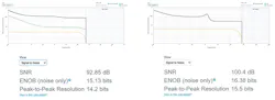
Precise measurement of DC and AC voltages is a fundamental requirement in industrial applications. In the application circuit shown in Figure 5, the external driver circuit is bypassed for the AD4134 and the voltage-source output is directly interfaced to the ADC input. As previously discussed, this is made possible by the resistive input impedance characteristic of CT sigma-delta ADCs.

In contrast, the AD7768-1, which utilizes a DT architecture, necessitates an external driver circuit to support its front-end S&H stage. The comparative results illustrated in Figures 6 and 7 demonstrate that the AD4134 delivers superior performance in SNR and ENOB across all tested scenarios, including DC, mid-frequency AC, and high-frequency AC voltage measurements.

Pressure Sensor Measurement
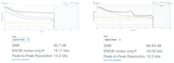
In pressure sensor measurement circuits (Fig. 8), an instrumentation amplifier (in-amp) must be employed as the primary stage. This requirement remains essential for the AD4134 because pressure sensors typically exhibit high source impedance, necessitating a high-performance front-end to maintain signal integrity.

As illustrated in Figure 9, the AD4134 continues to demonstrate superior SNR and ENOB performance compared to its DT counterpart in this application.
Current-Sense Measurement
Similarly, current-sense application often exhibits high source impedance, necessitating the use of an instrumentation amplifier in the primary stage (Fig. 10). As illustrated in Figure 11, the AD4134 continues to demonstrate superior SNR and ENOB performance in this application.


The table provides a comprehensive comparison between CT sigma-delta, DT sigma-delta, and SAR ADCs. From this comparison, it’s evident that CT ADCs offer numerous advantages, including higher operating bandwidths, simplified input signal-chain design, and enhanced electromagnetic-interference (EMI) immunity. However, certain design constraints remain, such as a more limited input common-mode voltage range.

Ultimately, engineers must evaluate specific system requirements to select the ADC architecture that best aligns with their design goals.
Conclusion
The following conclusions can be drawn from the analysis and simulation results. In many precision industrial measurement applications, CT sigma-delta ADCs eliminate the need for com-plex, high-order front-end AAFs due to their inherent filtering characteristics.
The higher operating bandwidth of CT sigma-delta ADCs significantly broadens their range of applications. This enables them to handle signals that were previously beyond the reach of traditional sigma-delta architectures.
The resistive input impedance of CT sigma-delta ADCs removes the requirement for high-speed, high-precision op amps as driver circuits, leading to substantially reduced PCB footprint and overall design costs.
For signal sources with high-source impedance, an instrumentation amplifier remains necessary between the source and the ADC. Failing to do so will result in a loading effect, causing signal attenuation and measurement errors. CT sigma-delta ADCs offer a more straightforward approach to implementing multi-device synchronization, which is critical for simultaneous sampling in complex industrial systems.
>>Download the PDF of this article
About the Author
James Cheng
Field Applications Manager, Analog Devices Inc.
James Cheng, a field applications manager at Analog Devices, has a background in audio, ATE, and automation products. He joined ADI in 2014 as a field applications engineer and supported audio. Since 2018, he’s expanded his expertise in working on ADI’s industrial products, supporting ATE and automation customers’ engagements.
Comment About the Article
To join the conversation, and become an exclusive member of Electronic Design, create an account today!

Leaders relevant to this article: