Q&A: Turning New Designs into Reality Through Innovative Manufacturing
This file type includes high-resolution graphics and schematics when applicable.
Manufacturing plays a critical role in today’s fast-paced design environment. Designers and manufacturers in the microelectronics industry face major challenges. Getting some help can reduce costs, improve time to market, and boost product quality.
Orbotech helps deliver enhanced production solutions for manufacturers of printed-circuit boards, flat-panel displays, advanced packaging, microelectromechanical systems, and other electronic components. I talked with Asher Levy, Chief Executive Officer, about Orbotech and the challenges faced by designers and manufacturers.
Wong: Due to consumer-driven demand for increased functionality and faster times to market, designers of new electronic devices are now looking to production to ensure product success. Have you seen significant changes in the relationship between design and production in the industry?
Levy: As smartphones and other electronic devices become smaller, slimmer, and faster with almost unlimited features, technical pioneers, product designers, and global brands require new technologies and processes from manufacturing service providers and equipment suppliers to enable more complex functionality and in smaller form factors.
The brands that succeed will be from companies that leverage new manufacturing equipment to increase manufacturing capacities so that they can produce smaller, low-cost electronics-based solutions in high volume in anticipation of future demands.
Wong: What do you see as the major challenges facing designers and manufacturers in the microelectronics industry?
Levy: Designers and manufacturers are faced with solving increasingly complex designs inside smart devices and their accompanying infrastructure requirements, while maintaining the flexibility to react to the fast-changing demands of the consumer-driven market.
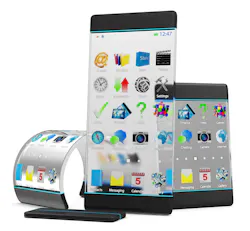
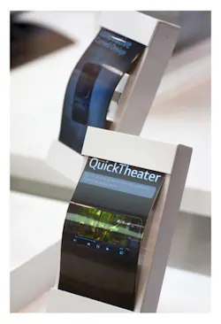
Many obstacles exist in the pipeline between the device designer and the manufacturing floor. For example, if you’re manufacturing a smart watch, how do you accommodate an array of sophisticated MEMS on a curved surface? Can you properly connect the advanced packages necessary to perform the myriad functions expected from such a device? What’s the best substrate to use? Do you have the proper inspection and repair systems in place to assure high yield and quality?
Orbotech solves multiple challenges that arise in the potential disconnect between a design and its realization, and not just about producing capital equipment. We consider the broader scope of the manufacturing environment to help manufacturers meet any design challenge thrown at them.
Wong: Your website claims that Orbotech’s solutions have helped produce virtually every electronic device in the world. How is this so?
Levy: Orbotech provides a broad offering of mission-critical solutions that serve product designers, global brands, and electronics manufacturers. With the overall breadth of our technological competencies and leading systems, Orbotech transitioned from a solution supplier to an enabler of new design concepts, from an equipment vendor to a full-fledged process innovator that makes a significant impact on the electronics manufacturing environment.
With this breadth of electronics manufacturing touch points, we can comfortably say that every fabricator in the world is using one or more of Orbotech’s solutions.
Wong: What role do you see Orbotech playing in supporting the fast-paced electronic design industry? How does manufacturing play a significant role?
Levy: The electronics industry certainly needs to support miniaturized electronics packages, new form factors, and different substrates. In 2014, to accommodate this need, we acquired SPTS, a leading supplier of etch and deposition process equipment for the global semiconductor- and microelectronic-device manufacturing industries. SPTS was a crucial strategic piece that expanded our offering even further into the realm of “electronics connecting,” enabling increasingly smaller and more sophisticated components to be implemented within the most challenging smart-device designs.
But well before the acquisition, Orbotech launched a strategic exploration process that took a long view of the electronics landscape to identify new growth areas where we could make our impact in next-generation device design and manufacturing. We identified several areas of transition in which we decided to invest our efforts.
Orbotech expanded its offerings from inspection, verification, and yield-enhancement or “electronics reading” solutions to being a significant player, through the acquisition of SPTS, in the semiconductor arena. We also have an extensive array of groundbreaking solutions for automated optical repair for both PCB and FPD manufacturing environments.
Wong: Name some of the Orbotech’s most significant manufacturing solutions and explain how they help device manufacturing.
Levy: Our direct imaging solutions for high-volume manufacturing environments are capable of imaging on almost every photo-resist type. These solutions represent a major breakthrough in quality mass production, generating up to 7000 panels per day. They provide PCB manufacturers with ultimate flexibility by providing a fully automated in-line solution that uses the most advanced imaging technologies available regardless of the substrate, while reducing their total cost of ownership.
Flat-panel repair systems like Orbotech’s Prism offers state-of-the-art repair capabilities to support production of the most advanced display technologies, including OLED displays. This is the essence of process innovation, because it’s a true game changer. In the past, ablation—the removal of excess deposed metal—was performed manually by removing a panel from the assembly line and literally scraping off excess with a knife. Beyond being a slow and inefficient process, it also could potentially damage the unit, which ultimately impacts yield. By combining both deposition and ablation in a single automated solution, Prism represents a total transformation of the flat-panel repair process since it leaves no room for error.
Automated optical shaping systems for PCBs also combine short and open repair capabilities in a unified high-yield system, again representing a significant innovation in how actual manufacturing processes are conducted in the electronics manufacturing environment.
Wong: What do you see for the future of micro-electronics manufacturing, and what kinds of advances can we expect to see from designers as the result?
Levy: First, we need to understand that if, in the past, electronics manufacturers dictated the boundaries of what is or isn’t possible from a production standpoint, today’s agenda is being driven by new advances in science, engineering, and device design. The introduction of wearables, smart glasses, and watches poses significant challenges to every link in the electronics manufacturing ecosystem—especially in terms of translating designs that take their inspiration from Star Trek into functioning intuitive products that have the intended “wow” effect for end users.
And that’s just the tip of the iceberg. We’re looking at the manufacturing opportunities available for the myriad new possibilities on the horizon—the inter-connectability of devices and systems that will hasten the arrival of the next stage in electronics: the Internet of Things, the smart home, the self-driving or “autonomous” car, next-generation medical devices, wearables.
Looking for parts? Go to SourceESB.
About the Author
William G. Wong
Senior Content Director - Electronic Design and Microwaves & RF
I am Editor of Electronic Design focusing on embedded, software, and systems. As Senior Content Director, I also manage Microwaves & RF and I work with a great team of editors to provide engineers, programmers, developers and technical managers with interesting and useful articles and videos on a regular basis. Check out our free newsletters to see the latest content.
You can send press releases for new products for possible coverage on the website. I am also interested in receiving contributed articles for publishing on our website. Use our template and send to me along with a signed release form.
Check out my blog, AltEmbedded on Electronic Design, as well as his latest articles on this site that are listed below.
You can visit my social media via these links:
- AltEmbedded on Electronic Design
- Bill Wong on Facebook
- @AltEmbedded on Twitter
- Bill Wong on LinkedIn
I earned a Bachelor of Electrical Engineering at the Georgia Institute of Technology and a Masters in Computer Science from Rutgers University. I still do a bit of programming using everything from C and C++ to Rust and Ada/SPARK. I do a bit of PHP programming for Drupal websites. I have posted a few Drupal modules.
I still get a hand on software and electronic hardware. Some of this can be found on our Kit Close-Up video series. You can also see me on many of our TechXchange Talk videos. I am interested in a range of projects from robotics to artificial intelligence.
Voice Your Opinion!
To join the conversation, and become an exclusive member of Electronic Design, create an account today!

Leaders relevant to this article:


