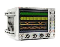
To date, no manufacturer has adopted the stratospheric-bandwidth oscilloscope (SBO) terminology, although several very high frequency oscilloscopes, such as Keysight Technologies’ 63-GHz Z-Series Infiniium DSOZ634A shown in Figure 1, clearly could support the SBO description. We already have variations on the digital storage oscilloscope (DSO) such as MSO mixed-signal (now generic, but began by Hewlett Packard in 1995), digital-phosphor (DPO) and mixed-domain (MDO) from Tektronix, and high-definition (HDO) from Teledyne LeCroy. Why not an SBO?
Courtesy of Keysight Technologies
A common aspect that distinguishes today’s SBOs from other scopes is their use of semiconductor technologies that cannot directly support the claimed bandwidths. A very high-end oscilloscope takes a few years to develop, so no matter what speed IC process it uses, at the time it is introduced, the frequencies it needs to work with have become even higher. It’s not possible to keep up.
Instead, each manufacturer making these scopes has figured out how to split the input signal spectrum into pieces small enough to handle with existing IC technology. Of course, they also had to develop the means to reassemble the original signal by combining outputs from the separate paths.
This approach should not be confused with time-interleaved sampling (TIS), which has been used by many scope vendors to increase time resolution. A common way that this technique has been presented to users was to specify a scope’s longer memory and higher sample rate when multiple channels were combined.
The concept of TIS is easy to understand, but TIS designs only work well when inherent performance limitations are addressed. Because a single tone is converted by all n ADCs being interleaved, the gain and group delay of each path contribute distortion to the degree that the n paths differ. So, additional compensation must be included to normalize the gains and align the path delays before the separate outputs can be combined. Of course, gains and delays are frequency- and temperature-dependent.
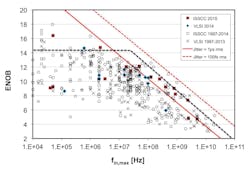
Another significant limitation is caused by the ADC clock jitter. A 2015 Ph.D. dissertation1 presents a plot of input frequency vs. achievable ENOB for ADCs described in ISSCC and VLSI Symposium papers. As shown in Figure 2,1 there is a maximum frequency at which the quantization errors associated with a certain ENOB are overtaken by sampling clock-related errors—aperture jitter. The paper concludes that rms jitter less than 100 fs is needed to achieve an ENOB of 6.0 at input frequencies higher than 20 GHz.
Courtesy of S. Callender
The paper also examines the benefits of a frequency-interleaved approach relative to one using TIS. Splitting the input spectrum into two or more parts has the benefit of allowing the ADCs in each path to operate at lower clock rates, which reduces sensitivity to sampling clock jitter. On the other hand, downconverting higher-frequency bands to baseband involves mixing with a suitable local oscillator (LO). Unless LO noise is low, the improvement in sensitivity to sampling clock jitter could be offset by the LO noise that gets added to the input signal.
Commercial solutions
In a 2010 technical brief,2 Peter Pupalaikis, vice president of technology development at Teledyne LeCroy, discusses the spiraling costs encountered as oscilloscope companies pursued higher bandwidth direct-sampling designs, which required “… the redesign of various custom ICs, with costs increasing at an exponential rate. As the life-cycle of these high-performance instruments continues to shrink, these costs are passed on to oscilloscope customers.”
And, as described in a 2013 article3 by Brig Asay, at the time product manager of high-performance oscilloscopes at Agilent Technologies’ oscilloscope product division, “… the need for higher oscilloscope bandwidths is outstripping what can be achieved with … [a direct-sampling] architecture, even when very fast semiconductor processes are used to realize the circuits…. Some of the high-bandwidth oscilloscopes have employed variations of what are sometimes called hybrid filter bank (HFB) techniques. Basic HFB uses analog bandpass filters to select and redirect separate frequency bands.”
Digital bandwidth interleave
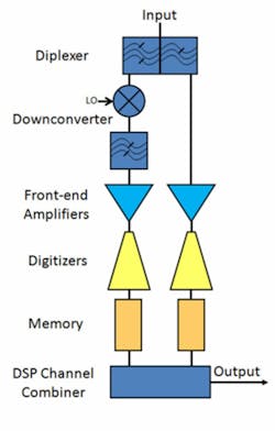
The solution that LeCroy developed before being acquired by Teledyne—digital bandwidth interleave (DBI)—uses a diplexer to split the input spectrum into lower and upper bands (Figure 3). Only two bands are considered here, but the technique can address three or more bands if required. The lower band contains frequencies within the bandwidth of the front-end amplifier and ADC. The higher band is mixed with an LO to translate it to baseband, and in the process, it becomes spectrally reversed.
Courtesy of Teledyne LeCroy
In the 30-GHz example discussed in another LeCroy DBI paper,4 two bands are developed—DC to 16 GHz and 16 GHz to 30 GHz. After downconverting the upper band, both are sampled at 40 GHz. The paper continues, “… alternate zeros [are inserted] into the waveforms in both bands. This process upconverts the sampling rate to 80 GS/s. This also is equivalent to mixing the signals with a 40-GHz local oscillator, and as a result, we image the baseband spectra about 40 GHz and harmonics thereof. At this point, we low-pass filter the signals in both bands, and we are left with the baseband spectra and a new Nyquist frequency of 40 GHz due to the 80-GHz sampling rate.”
To recover the upper band, which still is spectrally reversed, the paper states, “We mix the high band with a local oscillator [31.25 GHz] in order to remove the spectral reversal and also to restore it to its original frequency range. The output of this mixer is bandpass filtered eliminating the upper sideband image….”
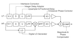
Clearly, LeCroy’s DBI approach is technically sound, as has been demonstrated in several scope models such as the LabMaster 9 Zi-A and 10 Zi-A scopes, the latter series with bandwidths to 100 GHz. Nevertheless, as shown in Figure 4,5 recombining the multiple bands is far from straightforward. Several types of errors have accumulated during the splitting, downconversion, and filtering.
Courtesy of Teledyne LeCroy
One factor, the delay correction, is partially caused by the baseband and upper-frequency paths being different. And, in the 30-GHz example, each path was sampled at 40 GHz, which was achieved by time interleaving a few slower speed ADCs. So, interleave correction is necessary for each of the composite ADCs.
These are just a couple of the calibration and compensation algorithms—the “secret sauce” that underlies any of the various SBO techniques and provides amplitude and phase accuracy in the combined-band output that is comparable to the performance of a conventional single-band lower-frequency scope.
Asynchronous time interleave
Tektronix has developed the asynchronous time interleave (ATI) bandwidth-multiplication technology used in the 70-GHz Model DPO70000SX. The overall scheme is similar to DBI to the degree that two paths are processed and combined to form the higher bandwidth output. However, there are several distinct differences as well.
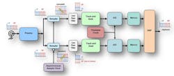
As discussed in a 2015 white paper6 and also in a 2016 patent,7 ATI signal processing (Figure 5) drives two identical paths rather than immediately forming upper and lower bands as with DBI. One result of this architecture, as claimed in the white paper, is reduced noise power spectral density because the noise is spread across the total sample rate, which is twice the sample rate of the individual ADCs.
Courtesy of Tektronix
The two paths are distinguished by the phase of the asynchronous pre-sampler clock—one clock (C’) is 180 degrees different in phase with respect to the other (C). The frequency of both is above the final bandwidth. In the 70-GHz example described in reference 6, a 75-GHz pre-sampling clock is used, resulting in a 37.5-GHz Nyquist frequency.
If you consider a signal consisting of frequency A that is less than Nyquist and a tone B that is greater than Nyquist but less than frequency C, what happens when the signal is sampled by clocks C and C’? Because frequency A is less than Nyquist, it is retained as a baseband signal. In addition, frequencies A and B are mixed with the sampling frequency C and C’. Mixing is equivalent to multiplication, and if each signal component and the sampling frequency are sine waves, after low-pass filtering at 37.5 GHz, one path will contain the original sin (A) term and –cos (C-B). The other path will have the same sin (A) term but +cos (C-B).
The C-B term is equivalent to the reversed-spectrum upper DBI band. However, because frequency B lies between Nyquist and the presampling frequency C, C-B clearly has aliased to a position within the baseband from DC to Nyquist—there’s nothing to restrict frequency A from falling at the same location.
Ordinarily, the creation of an alias is something to be avoided in any data acquisition or processing scheme. In ATI, it occurs in both paths, which allows it to be removed. The aliasing and 180 degrees phase difference are shown in Figure 4 so cancellation is implied. However, unless you go through the math, it’s not obvious from the figure how the DSP can recover the upper frequency band.
After conversion by ADCs running at a rate unrelated to the pre-sampling clock—100 GHz in the white paper6 example—the paths are resampled at exactly the same C and C’ frequency and phase used in each path’s respective pre-sampler. The two paths now contain the original baseband sin (A) but have gained a sin (B) term. One path also has a cos (C-B) term and the other a –cos (C-B) term. Summing the two paths cancels the cos (C-B) terms and results in sin (A) + sin (B)—the original signal, although the amplitudes may need adjusting. Higher frequency terms also are created by the resampling but are removed by a low-pass filter at the 75-GHz sampling frequency.
Similar to DBI, ATI recovers the upper band by mixing with a high-frequency LO—75 GHz instead of LeCroy’s 31.25 GHz. In both cases, mixing serves to restore the upper band’s original spectrum. DBI always works with physically separate frequency bands, so the downconverted upper band doesn’t add to the baseband spectrum. In ATI, aliasing does occur but is cancelled when the paths are combined after resampling at the original pre-sampling frequency and phase. Most importantly, in both DBI and ATI the upper-band restoration is done digitally so there is no limit to the frequencies that can be handled if the RF signals ahead of the ADCs have sufficient fidelity.
Figure 14 of reference 7 includes a compensation oscillator and a means to switch it in place of the input signal. The patent discusses details of one embodiment of the oscillator that explicitly provides a “… relatively large and linear tuning range compared to varactor tuning at these frequencies. The large tune range is helpful to overcome process modeling uncertainty and process variability.” Both amplitude and phase can be compensated. In particular, the compensation oscillator supports good phase and amplitude correction in the cross-over region at the top of the baseband and the bottom of the upper band.
RealEdge technology
Not a lot has been published about Keysight’s RealEdge—a third SBO technology in addition to DBI and ATI. As Agilent’s (now Keysight’s) Asay explains in reference 3, “Agilent began shipping its RealEdge technology in 2012 when it moved from its previous 33-GHz products to the 63-GHz models of the 90000 Q-Series Infiniium scopes. The RealEdge architecture consists of a proprietary combination of the basic TIS and HBF techniques.”
Variations of this wording are used in several recent Keysight scope datasheets; for example, according to the Q-Series datasheet, “RealEdge technology uses custom chips to seamlessly increase the bandwidth of Q-Series oscilloscopes.” And from the Z Series datasheet, “RealEdge technology is implemented using a unique combination of time interleaving, frequency interleaving, and proprietary signal processing.”
Verifying an SBO’s accuracy
Having enough bandwidth is essential for applications involving some of today’s fastest data communication rates. But, bandwidth alone isn’t useful unless a scope also addresses amplitude and phase accuracy as well as noise level. As discussed by Patrick Connally, product manager at Teledyne LeCroy, “Viewing the shape of an oscilloscope’s step response demands a signal source that is significantly faster than the instrument—the rise time measured by the scope is the root-sum-of-squares of the rise times of the signal and of the scope itself.”
He continued, “Things began to get really interesting when we were developing the LabMaster 10-100Zi-A. It’s the first and only real-time oscilloscope with 100 GHz of analog bandwidth, which means it has a 20-80 rise-time of just 3.5 ps. Electrical signal sources that are suitable to characterize that just don’t exist, so we use an extremely fast (hundreds of fs) optical impulse signal and a high-bandwidth photodetector. This creates a very fast electrical impulse, which we can mathematically integrate to get a step response.”
Tek’s David Taylor, Sr., technical marketing manager, performance instruments, also mentioned an optical test method. He said, “For NIST traceability, Tektronix recommends using one of the laser diode sources referenced by NIST, which can produce impulses capable of characterizing test equipment to 100 GHz and beyond. The NIST laser diode-based test could be done by any users sophisticated enough to be developing relevant optical and electronic systems with signaling approaching the rise time of the scope.
“Although pulse response is not specified in Tek’s high-performance scopes, we thoroughly characterize the time-domain performance and accuracy of our scopes to ensure operation within their design parameters, including impulse and step response,” he continued. “We generally use a math function to integrate impulse response measurements into the corresponding step response visualization. This characterization is done both in engineering and in manufacturing.”
And, Keysight’s Asay, Infiniium marketing manager at the company, explained that, “Inside all [Keysight] oscilloscopes is a performance verification test, which can be used to confirm the bandwidth of the scope to the NIST standard. In addition to this, it is relative easy to perform noise and jitter tests on the oscilloscope.”
Using an SBO
In common with other SBOs and following a well-established trend in the industry, Keysight’s high-performance scopes have a very large number of built-in features as well as a long list of options. For example, as the datasheet for the Series Z Infiniium scopes states, “EZJIT Plus automatically detects embedded clock frequencies and repetitive data patterns on the oscilloscope inputs and calculates the level of data-dependent jitter that is contributed to the total jitter PDF by each transition in the pattern….”
EZJIT, EZJIT Plus, and EZJIT Complete jitter analysis software are three of at least 17 analysis software applications available for the Z Series scopes. In addition, 32 compliance test and validation applications can perform standard tests on buses such as BroadR-Reach, DisplayPort 1.2, MOST, or USB 3.1. Optional protocol decoding software from generic 8b/10b to multiple MIPI and USB versions also is compatible with the Z Series.
If you regularly work with standards such as SAS-3, 28/32G FibreChannel, or MIPI M-PHY, you really do need an SBO. A table in the Keysight Z-Series datasheet lists preferred scope bandwidth as a function of bus speed. The table’s a big help because it’s not always the data rate that determines the needed bandwidth: rise time also plays a role. For example, the SAS-2 standard has a 6-Gb/s data rate but only a 42-ps rise time and requires a 16-GHz bandwidth. In contrast, the MIPI M-PHY standard has a similar 5.83-Gb/s data rate but a much faster 17.2-ps rise time. It needs a 24-GHz bandwidth.
Some of the changes to your test method required when using an SBO include applying the correct torque to RF connectors, compensating for cable losses, and employing the correct probe with the right probing technique. Tek’s Taylor commented, “At RF/microwave frequencies, consistency of the measurement setup is critical. Tek’s TriMode probes allow a single probe tip to be soldered into the system under test, supporting single-ended, differential, and common-mode measurements … without changing or disturbing the probe tip or node under test.”
On the other hand, you don’t get any points for using an SBO when you don’t need one. As Keysight’s Asay noted, “On a fast oscilloscope, with a signal that has a slow rise time, it’s very easy to underestimate the scope noise floor in the measurement. You really do need to get the right scope bandwidth for the signal.” This is another way of saying that a scope’s noise is integrated over the entire bandwidth—and for an SBO, that’s a lot of Hertz. If you only need to measure a 1-GHz signal, even a 30-GHz SBO will add noise over 29 more gigahertz than necessary.
References
- Callender, S., Wideband Signal Acquisition via Frequency-Interleaved Sampling, Ph.D. Dissertation, UC Berkeley, 2015.
- Pupalaikis, P., Digital Bandwidth Interleaving, LeCroy, Technical Brief, April 2010.
- Asay, B., “Architectures for ultra-high-performance scopes,” Electronic Products, June 14, 2013.
- The Interleaving Process in Digital Bandwidth Interleaving (DBI) Scopes, LeCroy, White Paper, December 2009.
- Pupalaikis, P., “Recent Advances in Waveform Digitizer Technology,” North Jersey Section MTT-Society & AP Society Joint Chapter 24th Annual Symposium and Mini-Show, October 2009.
- Techniques for Extending Real-Time Oscilloscope Bandwidth, Tektronix, White Paper, March 2015.
- Knierim, D. G. and Lamb, J., S., “Test and measurement instrument including asynchronous time-interleaved digitizer using harmonic mixing,” U.S. Patent 9,306,590 B2, April 2016.
About the Author

Tom Lecklider
Voice Your Opinion!
To join the conversation, and become an exclusive member of Electronic Design, create an account today!

Leaders relevant to this article:

