Why Communications Systems are Migrating to ASIC Architectures
What you'll learn:
- How ASIC architectures cut power consumption and ease thermal constraints compared with FPGA-based communications designs.
- The ways that tighter mixed-signal and RF integration in ASICs improve system efficiency, beamforming, and overall radio performance.
- Why long-term reliability, radiation tolerance, and lifecycle management are pushing advanced 5G, 6G, and satellite systems toward custom silicon.

Across 5G infrastructure, emerging 6G platforms, satellite payloads, microwave backhaul, and non-terrestrial-network (NTN) systems, silicon architecture is increasingly becoming a defining system constraint (Fig. 1). As bandwidth increases, antenna counts rise, and modulation schemes grow more complex, power density, integration efficiency, and thermal limits determine what can realistically be deployed — not simply what’s functionally achievable.

FPGAs remain highly effective during early development and amidst evolving standards. Their reconfigurability allows engineering teams to absorb specification changes and accelerate time-to-prototype.
However, once functional requirements stabilize and production volumes rise, optimization priorities shift. Power efficiency, mixed-signal integration, and long-term reliability move to the forefront. At that stage, many communications systems transition from programmable logic to application-specific integrated circuits (ASICs), because the architectural tradeoffs increasingly favor fixed-function silicon (Fig. 2).
Power as the Dominant Constraint
In current-generation communications silicon, total device power is largely driven by two contributors: the programmable logic fabric and the processor subsystem. As signal-processing workloads scale — particularly beamforming, fast Fourier transform (FFT) / inverse FFT (IFFT), filtering, and channelization — the efficiency of the underlying architecture becomes critical.
In FPGA-based designs, the programmable fabric introduces inherent overhead. Look-up tables (LUTs), routing networks, DSP slices, embedded memories, and clock-distribution resources carry significantly higher switched capacitance than fixed ASIC logic. Configuration memory and unused routing resources remain present regardless of utilization, contributing both static and dynamic losses. As a result, power doesn’t scale linearly with useful computation.
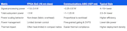
A representative communications implementation on a 16-nm FPGA SoC such as the Zynq UltraScale+ — using approximately 85k LUTs, hundreds of DSP blocks, and operating between 100 to 250 MHz — typically dissipates 1.6 to 2.4 W in programmable logic alone. Additional losses arise from wide data paths crossing clock regions and from configuration infrastructure. In compact radios or small-cell platforms, this quickly becomes a thermal constraint rather than a secondary optimization.
An ASIC implementation removes this structural inefficiency (Table 1). Multiply/accumulate arrays are hardened, data paths are physically localized, and routing is constrained to minimize capacitance. Clock and voltage domains are defined according to workload characteristics rather than architectural generality. For equivalent functionality, logic power typically falls to approximately 0.35 to 0.60 W at 12 nm and 0.25 to 0.40 W at 7 nm, representing a 4X to 10X reduction.
It’s also worth noting that TSMC 12-nm technology is an optical shrink of 16 nm, typically delivering on the order of 10% to 20% logic power reduction and approximately 15% to 25% area reduction, while maintaining broad compatibility for analog IP such as phase-locked loops (PLLs) and data converters. This allows for incremental power improvement without requiring a wholesale redesign of mixed-signal subsystems.
Processor subsystems show smaller deltas at equivalent nodes. FPGA SoCs integrate hardened Arm Cortex-A53 and Cortex-R5 cores, so active CPU power is broadly comparable to ASIC implementations. A communications workload comprising quad Arm Cortex-A53 at ~1 GHz plus dual Arm Cortex-R5 for real-time control typically consumes approximately 0.9 to 1.4 W in a 16-nm FPGA device. Node scaling in ASIC implementations reduces that modestly.
The more significant difference lies in power-management flexibility. Custom silicon enables fine-grained power gating, domain-level dynamic voltage and frequency scaling, independent voltage islands, and deep retention states. In burst-oriented communications traffic profiles, these techniques materially reduce idle and standby consumption.
When CPU and programmable logic are combined, representative FPGA-based communications subsystems may approach approximately 3 W total dissipation, whereas comparable ASIC implementations at 12 nm or 7 nm can operate closer to 1 to 1.25 W. This difference materially alters thermal design constraints and deployment flexibility.
Integration and Deterministic Performance
Power is only one dimension of the migration. Integration increasingly determines overall system efficiency.
FPGA-based platforms frequently rely on off-chip ADCs and DACs connected via high-speed serial interfaces such as JESD204. While functionally effective, these links introduce measurable interface power, additional clocking overhead, and board-level signal integrity constraints.
In a custom ASIC, converters can be architected specifically for the required resolution and sampling rate. Sub-6-GHz radios typically require 12 to 14 bits at 100 to 250 MSPS, while wideband millimeter-wave (mmWave) systems operate at 10 to 12 bits and 1 to 3 GSPS.
Compared with discrete broadband converters, application-specific integrated ADC and DAC architectures can materially improve energy efficiency (often multiples, depending on resolution/bandwidth/architecture) and lower system power by eliminating high-speed chip-to-chip I/O.
Further integration of RF functions, including LO generation, mixers, gain stages, and filtering, shortens signal paths and reduces parasitics. Improved gain and phase alignment directly benefits beamforming coherence. Near-RF and direct-sampling architectures can remove intermediate frequency stages entirely, reducing bill of materials and simplifying calibration. Although direct-sampling ADCs may draw higher instantaneous power, they often reduce overall architectural complexity and latency.
Embedded FPGA (eFPGA) fabric can provide limited post-deployment flexibility, but it consumes significant silicon area and is less power-efficient than fixed-function logic. For high-throughput data paths such as filtering, FFT, or forward error correction, hardened logic or licensable DSP cores typically deliver superior performance per watt. As such, eFPGA is best viewed as a controlled flexibility mechanism rather than a substitute for optimized signal-processing hardware.
Reliability Beyond Development Environments
In terrestrial infrastructure, predictable thermal behavior and long service life are essential. In space-based systems, reliability requirements intensify further.
Low-Earth-orbit and medium-Earth-orbit (MEO) payloads must tolerate latch-up, single-event effects, and extended temperature cycling. ASIC implementations support radiation-hardened-by-design techniques such as hardened flip-flops, triple modular redundancy, and carefully engineered bias networks (Fig. 3). Guard-ring structures and rad-aware layout reduce susceptibility to parasitic conduction paths.

In addition, ASIC implementations can leverage radiation-hardened packaging technologies not available in commercial off-the-shelf FPGA devices.
Partitioning for Long-Term Scalability
Many communications architectures now separate Layer 1 signal processing from higher-layer protocol functions. A communications ASIC implements converter interfacing, beamforming, FFT/IFFT processing, filtering, forward error correction, and PHY timing, while a companion application processor handles Layer 2/3 stacks, control-plane logic, and security functions.
High-speed interconnects such as PCIe Gen4 or Gen5 enable scalable chip-to-chip partitioning. This separation allows the communications ASIC to maintain a 10- to 15-year lifecycle without aggressive node migration, while the application processor continues to benefit from process scaling and improved performance per watt. System-level power can therefore continue to decline without redesigning the core signal-processing silicon.
In aggregate, these architectural differences frequently translate into overall system-level power reductions of 2.5X to 5X, alongside tighter mixed-signal integration and improved long-term reliability. As bandwidth, antenna count, and deployment density continue to increase, these factors become structural requirements rather than incremental improvements.
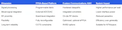
FPGAs remain critical during exploration and early deployment. However, at production scale, custom silicon increasingly defines the power-efficient and architecturally sustainable foundation for advanced communications infrastructure (Table 2).
>>Download the PDF of this article

About the Author
 Ian Lankshear
Ian Lankshear
CEO, EnSilica
Ian Lankshear, CEO of EnSilica, co-founded the company in 2001. Under his stewardship, the company has enjoyed sustained growth based on market-led opportunities, innovation, and export success. He has a strong technical and commercial background covering semiconductors and adjacent markets.
Ian’s early career was in radar systems development for Siemens Plessey Systems. He moved into semiconductor development in 1996, working for Hitachi and then for Nokia. Ian holds a First-Class Honors degree in Electrical & Electronics Engineering.
Comment About the Article
To join the conversation, and become an exclusive member of Electronic Design, create an account today!
 Leaders Logo
Leaders relevant to this article: