NAND Rises to the Occasion in Data-Heavy IoT Applications

Download this article in PDF format.
Long a staple of consumer devices such as MP3 players, digital cameras, and USB flash drives, nonvolatile NAND flash memory is raising its game to respond to the new challenges posed by data-heavy Internet of Things (IoT) applications (Fig. 1). IoT applications for NAND flash cover a breathtaking range: industrial automation and Factory 4.0, connected vehicles, wearables, healthcare, aviation, plus just about any application that begins with “smart”: smart metering, smart homes, smart utilities, smart farms, smart logistics, and more.

1. NAND flash memory finds a home in numerous data-heavy IoT applications. (Source: Delkin Devices)
Turning on the channel requires a threshold voltage VT to be applied to the control gate. If the floating gate is already charged, its effect is to increase the required threshold voltage to VT+; otherwise the required value of VT is a lower value, VT-. To read a cell, the controller applies an intermediate voltage between VT- and VT+. If the channel conducts, the floating gate is uncharged; otherwise, it’s charged.
Unlike other memory technologies, a NAND flash device can’t be reprogrammed at the individual byte level. Due to its architecture, it can only be read and programmed in pages—typically between 4 and 16 kB—and can only be erased in blocks that range from 16 to 512 kB in size. A block must be completely erased before being reprogrammed. This two-step process is called a “program/erase” (P/E) cycle. Repeated P/E cycles lead to the breakdown of the oxide layer within the floating-gate transistor cells and eventual failure. Thus, the endurance, measured in number of P/E cycles, is a key specification.
A NAND flash device requires an internal or external controller to implement error code correction (ECC), manage bad blocks, and perform wear leveling—a technique to increase endurance by counting writes and dynamically remapping blocks to spread writes more evenly. So-called “raw” NAND includes just the cells and requires an external controller. A fully managed NAND device integrates the controller.
NAND flash devices come in different varieties, classified by the number of bits that can be stored in a single cell: single-level cell (SLC) (Fig. 2), multilevel cell (MLC), triple-level cell (TLC), and quad-level cell (QLC).
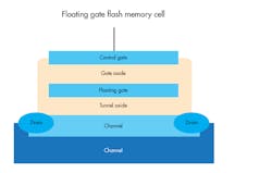
2. The structure of a typical single-level flash cell. (Source: Tech Target)
As Figure 3 illustrates, there’s a tradeoff between cell endurance and cell density: the higher-density cells have lower endurance.
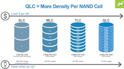
3. The designer can choose between several varieties of NAND flash to balance between endurance and density. (Source: Micron Technology)
More recently, manufacturers have begun offering three-dimensional (3D) NAND devices in MLC and TLC formats: current-generation 3D NAND devices stack up to 96 layers vertically for higher density.
Individual devices are available with capacities from 128MB to 2TB. Smaller-density devices are popular in consumer IoT applications such as wearables, smart appliances, set-top boxes, and smart TVs. High-density products find a home in cloud storage, plus data-heavy IoT applications such as gateways, factory automation, industrial PCs, surveillance, and drones.
There’s also a choice of interfaces. The embedded multimedia card (e.MMC) format uses an 8-bit parallel interface and integrates the flash memory and the controller into a 100-, 153-, or 169-ball-grid-array (BGA) package. The e.MMC version 5.1 specification has a 400-MB/s transfer rate.
The Universal Flash Storage (UFS) specification employs a full-duplex LVDS interface for higher transfer speeds than e.MMC. The latest (2018) UFS 3.0 revision uses two lanes to achieve a maximum total bandwidth of 2.9 GB/s.
NAND flash devices are offered in a variety of form factors, from single devices, to modules, to complete systems. Memory cards are used in both consumer and IoT applications; popular formats include USB flash drives, CompactFlash (CF), and secure digital (SD) cards in either standard or microSD sizes.
Solid-state drives (SSDs) combine large numbers of NAND flash devices and are popular as HDD replacements in both consumer and IoT applications. At the high end, a typical all-flash drive for cloud storage might be rack-mountable with 48 individual SSDs and a total capacity of 34 TB.
Picking the Right NAND for Your IoT Application
The IoT space covers a lot of ground, so there’s no “one size fits all” approach to picking a NAND solution. SLC NAND has the lowest density, but the highest performance and endurance. It’s preferred for high-end, mission-critical applications. MLC and TLC devices feature increasing density and lower endurance, and QLC devices are suitable for high-density, cost-sensitive mass-storage applications.
Consumer-oriented IoT applications can use off-the-shelf components, but many other IoT applications have specialized requirements. For example, security is a high priority for secure boot code, firmware, keys, and other sensitive information.

Standard commodity parts don’t include security features, but secure NAND flash devices offer volatile and nonvolatile block protection features. Volatile block protection locks one or multiple blocks until power is cycled; nonvolatile block protection permanently locks a fixed or variable range of blocks. Other security features include device-specific unique IDs, password protection, and AES256 data encryption.
Since some security features are computationally intensive, they’re typically included in a module-level design, e.g., a secure SSD.
An extended temperature range is important for IoT edge devices that are exposed to the elements or operate in a harsh industrial environment.

About the Author
Paul Pickering
Paul Pickering has over 35 years of engineering and marketing experience, including stints in automotive electronics, precision analog, power semiconductors, flight simulation and robotics. Originally from the North-East of England, he has lived and worked in Europe, the US, and Japan. He has a B.Sc. (Hons) in Physics & Electronics from Royal Holloway College, University of London, and has done graduate work at Tulsa University. In his spare time, he plays and teaches the guitar in the Phoenix, Ariz. area
Comment About the Article
To join the conversation, and become an exclusive member of Electronic Design, create an account today!

Leaders relevant to this article: