Wireless power applications are gaining popularity in many commodity products such as mobile phones chargers. Most of the wireless power solutions have focused on tight coupling with induction coil solutions at operating frequencies around 200 kHz, and Class E, F and S amplifier converter topologies. Recently, however, there has been a push for operation in the restricted and unlicensed lower ISM band at 6.78 MHz where traditional MOSFET technology is approaching its capability limit. Enhancement mode gallium nitride transistors offer an alternative to MOSFETs as they can switch fast enough to be ideal for wireless power applications. This article will focus on the experimental evaluation of an induction coil wireless energy system using Efficient Power Conversion’s (EPC) eGaN FETs in a half bridge topology operating at 6.78 MHz designed to be suitable for multiple 5 W USB based charging loads. The experimental system will further be compared to a similar unit based on equivalent MOSFETs in the power converter stage.
Wireless Energy
An induction wireless energy system is comprised of four main sections:
- Amplifier (a.k.a. a power converter)
- Transmit coil including matching network
- Receive coil including matching network
- Rectifier with high frequency filtering
To understand and design a wireless energy system, the designer must first understand the basic principle of operation of the transmit and receive induction coils.
The transmit coil is connected to a high frequency AC source such that it will generate a magnetic field that can couple to the receive coil, thereby transferring the energy. The induction coil set can be represented by a transformer circuit model with a high leakage inductance.
Fig. 1 shows the simplified schematic model for this transformer, where Lmx represents the magnetizing inductance, and Lrx represents the leakage inductance (where “x” refers to the primary, p, and to the secondary, s). Analysis of this model reveals that the ability to efficiently transfer power to the secondary is almost entirely determined by the primary side leakage inductance16. The high value of the leakage inductance in such systems, typically of the same magnitude as the magnetizing inductance, reduces the current in the primary circuit and thus the voltage across the ideal transformer primary winding. The leakage inductance is approximately proportional to the distance between the coils. The exact relationship between leakage inductance and distance between the coils falls outside the scope of this article, however, a coupling coefficient around 0.12 will be used in the design and discussion.
Operating the induction coils at resonance using external components significantly improves the transfer of power by increasing the voltage to the ideal transformer primary winding. This can be achieved by adding tuned matching networks to both transmit and receive coils16.
Operation in the ISM band at 6.78MHz requires an air core transformer as magnetic material losses would otherwise become significant. An air core transformer will have very low magnetizing inductance and hence requires higher currents to operate.
Given the need to operate at resonance and the transformer inductance values driven by the application, a matching network is required. This matching network will transform the impedance of the power stage to the transformer for maximum energy transfer, and will also be used to tune the resonant frequency of the coils to the desired frequency.
The induction coils used in this demonstration was designed and supplied by WiTricty Corp.5
Power Amplifier
Before selecting a power amplifier, the designer must first determine the main operating specifications, such as supply voltage and load power, as these will impact the choice of power topology. The goal is to design a system with the highest possible operating efficiency across the load variation.
EPC decided to evaluate a system that could operate up to 24 V to determine how much power could be efficiently transferred in a high frequency wireless system. Most USB applications are limited to 5 W, but market trends indicate that multiple loads driven by a single source are desired, which drives higher output power capability. Excluded in the demonstration is secondary regulation for the output to maintain 5 V regardless of load. Also excluded are the complexities of providing communications between the device and source modules for enhanced control and foreign metal object detection (FMOD) typical of wireless power systems.
Switching-based converters are required for wireless power applications because classic RF amplifiers do not have sufficient conversion efficiency to make them practical choices. This reduces the number of suitable converter choices for high efficiency wireless energy applications to Class D, Class E & F8 and Class S configurations9. To further add constraints, operation in the ISM band at 6.78 MHz12 is restricted to ±15 kHz bandwidth which essentially eliminates frequency modulation techniques for output regulation (voltage or load). Class E and F converters have the disadvantage that the main switch must be capable of blocking the full coil voltage whereas for Class D and S converters the switches only need to be able to block the supply voltage. Furthermore, class E and F converters are harder to control in applications where timing for ZVS operation is difficult to determine as the switch forms part of the resonant circuit. In the case of a class S amplifier, control requires a larger bandwidth than is permitted for use in the ISM band.
The logical amplifier selected was therefore a Class D converter operating at a fixed frequency. Duty cycle modulation will have little effect on output regulation if it is kept within ±10% of 50% duty cycle as the induction coils will be operating at resonance (The main effect of duty cycle will be to affect the efficiency of the converter outside the ±10% limits and will introduce current harmonics into the coil due to the spectral content of the source that may exceed general EMI limits).
The power amplifier chosen for evaluation was a half bridge, selected because eGaN FETs operate more efficiently at a higher voltage, and a high performance gate driver is available10 to keep costs down.
The converter is operated above resonance to take advantage of zero voltage switching (ZVS) and therefore obtain maximum power amplifier efficiency. The smallest 40 V eGaN FET, EPC2014, was chosen because it has a low on-state resistance and low Coss, all factors that will ensure minimum losses. Fig. 2 shows a block diagram of the wireless system.
Output Regulation and Control
There are two control methods used in wireless power converters:
- Constant bus voltage -varying frequency control
- Constant frequency -varying bus voltage control
Constant bus voltage with varying frequency control is the most popular method of control for wireless converters that typically operate in the 100 kHz to 200 kHz range. This control method is popular for wireless converters as it is results in a power converter with fewer components. However, it requires some form of feedback over the separation barrier for moderate control of the output. The traditional solution has been to use a form of digital communications protocol based on the wireless standard3. This offers a slow yet reasonable system for control. The main drawbacks of this method are:
- Communications between the device and source unit is superimposed on the power and can cause some perturbations in power. This may cause the system to not always operate at peak efficiency.
- The operating frequency varies to control the output based on load demand. When operating in the ISM band, this cannot exceed the maximum bandwidth of ±15 kHz and therefore consumes any tolerances in the coil design.
Enhanced output voltage regulation is achieved by adding a high performance buck regulator.
Constant frequency with varying bus voltage control is an alternative method of control for a wireless system that requires an additional front end converter to regulate the DC supply voltage to the power amplifier. The power amplifier, induction coil set and rectifier operate as a DC transformer. Additional regulation is still required on the output because the rectifier load will need to be operated as a constant resistor load to ensure maximum operating efficiency across the load range. This method allows very tight control of the operating frequency thereby meeting the strict ISM bandwidth requirements.
There are three types of wireless systems:
- Tightly coupled— source and receive coils are very close physically and the magnetic fields centered.
- Loosely coupled —source and receive coils are relatively close physically to each other but not necessarily touching, and the magnetic fields centered.
- Flexibly coupled17 —the distance between the source and receive coils and the magnetic field centers can vary). The loosely coupled coil system is investigated here.
Excluded from this method of control are the effects of varying distance and alignment between the source and device coils that will impact the coupling factor and hence the leakage inductance values of the equivalent circuit model transformer. This results in a shift of the resonant frequency of the coil. Methods to align and fix the distance between the coils are therefore highly recommended.
Rectifier
The function of the rectifier is to convert the high frequency AC of the receive coil to a DC voltage. Important considerations for the rectifier include conduction and switching losses. Synchronous rectification is possible, but requires additional consideration to correctly implement, given the critical timing needs when using eGaN FETs, the high switching frequency, and falls outside the scope of this article. The discussion here is therefore limited to a simple full wave diode bridge.
MOSFET Comparison
High frequency operation of the power amplifier means higher operating losses. It is preferable to operate the converter with zero voltage switching (ZVS) as this will yield maximum efficiency by eliminating Coss based losses. Determination of losses for each component in the circuit requires knowledge of how the circuit operates. Major loss contributors in the system are:
- Switching FETs including gate driver power consumption
- Rectifier diodes
- Induction coil set, including matching networks
To show what benefits eGaN FETs can bring to wireless energy it is necessary to compare the performance of the circuit when fitted with an equivalent MOSFET. The MOSFET selected is the BSZ130N03LS_G from Infineon13 and is available in a PG-TSDSON-8 (3 mm x 3 mm) package. It has a very similar RDS(ON) compared the EPC2014 but is only rated to 30 V where the eGaN FET is rated to 40 V.
A demonstration unit was designed and built to evaluate the performance of both the eGaN FET and the MOSFET. WiTricity Corp5 supplied the coils with matching networks.
The physical design of the circuit requires special attention to layout due to the high switching frequency of the converter and the rapid transitions in voltage and currents that can be present. The small size of the power circuit components makes measurements of critical nodes difficult, and therefore probes that allowed improved connection to oscilloscope probes were embedded into the PCB. An experimental unit was designed with four separate circuit boards:
- Source unit (power amplifier)
- Source coil
- Device coil
- Device unit (rectifier)
The source unit contains the power amplifier (switching converter), gate driver, supply regulators and a phase follower controller. Voltage of the source coil is fed back using a co-axial cable connection where it is converted into a square wave voltage. This square wave voltage is then delayed and timed before being used to drive the gate driver, producing a quasi-self-oscillating feedback controller for the system. This allows for very precise tuning of frequency, duty cycle, and dead-timing for each of the FETs. Fig. 3 shows the full wireless energy system setup. 50Ω SMA connectors were used to connect each of the boards together and 1 inch long nylon stand-offs were used to separate the source and device coils. The source coil feedback voltage connection made use of SMB snap-in connectors.
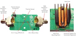
Fig. 4 shows a close-up of the source board with the heat-sink mounted for enhanced cooling of the eGaN FETs and MOSFETs. A single board was used to evaluate both the MOSFET and eGaN FET circuits side-by-side. The same source coil, device coil and device board was used during testing so that variations would be limited to only the differences in power amplifier switch technology.
A 15 mm by 15 mm by 14.5 mm high heat-sink made by Advanced Thermal Solutions14 was mounted flat on top of the eGaN FETs and MOSFETs using a thin sheet of Wakefield thermal interface material number 1737.
The LM5113 half bridge eGaN FET gate driver from Texas Instruments10 was used to drive both the eGaN FETs and MOSFETs. The small 2 mm x 2 mm BGA was selected for compactness. It is important to note that the LM5113 IC in this application is being operated well beyond its design frequency limit of approximately 5 MHz. The LM5113 logic circuits are capable of very high switching frequencies but the internal bootstrap power supply requires a minimum low-side on-time of about 100 ns to charge the high side supply to the required voltage. As a result, an additional external bootstrap power supply was added to the LM5113 circuit followed by a LDO regulator to ensure 5 V on the upper FET circuit. The high switching frequency also meant that the LM5113 would dissipate significant power and was therefore also placed under the heat-sink for additional cooling.
Fig. 5 shows a close-up of the device board with embedded shunt and minimum load for evaluation. Embedded Kelvin connections were used for accurate current and voltage measurements.
Experimental Results
Initial testing determined the optimal operating frequency for the coil set given various DC load resistances. It was determined that the peak operating point frequency given a fixed load of 23.6Ω was 6.639 MHz. Fig. 6 shows a graph of load power as function of efficiency including the power consumption of the gate driver circuit for the eGaN FET and MOSFET versions of the power amplifier and having a fixed load resistance of 23.6Ω and operating at 6.639 MHz.
Fig. 7 shows waveforms at 22 V for the eGaN FET setup and Fig. 8 shows waveforms for the MOSFET setup. The waveforms shown are lower gate voltage (cyan), switch-node (purple), source coil input current (green) and, device coil output voltage (yellow). The coil current was measured using a Rogowski Coil current probe made by Athena Energy11. The pick-up sensor was looped around one of the matching inductors on the coil set.
The system can operate with convection cooling, as shown in Fig. 9, up to a voltage of 20 V (12.5 W load power). At beyond 20 V, forced air cooling was required to keep one of the matching network inductors from exceeding 150°C.
Analyzing Losses
A loss breakdown analysis was performed for both the eGaN FET and MOSFET versions of the wireless boards and is shown in Fig. 10. Losses were determined for the switching FETs (conduction and switching), gate driver, source board (primary coil), device coil (secondary coil), and rectifier (conduction and capacitive).
Based on the device measurements at 22 V supply and load of 15 W, the following can be deduced:
- Induction coil set efficiency is 87.3%
- eGaN FET-based system efficiency is 82.9%
- MOSFET-based system efficiency is 78.8%
- Rectifier efficiency is 93.6%
Using eGaN FETs in the power amplifier yields a 4% amplifier efficiency improvement over the MOSFET version (a 24% reduction of power losses).
The key to high efficiency operation for a wireless energy system operating in the 6.78 MHz ISM band is to load the rectifier with a fixed resistance. This can be achieved by loading the rectifier with a buck converter whose input is programmed to operate as a fixed resistor while regulating the output voltage according to load requirements.
Finally, it should be noted that the eGaN FET devices used in the evaluation are too large for this application at a 5 W power level. The device chosen was based on the smallest product currently available in EPS’ family range. The devices tested yielded a 15 W load; however, smaller 30 V rated devices could be used for lower power levels with higher efficiency. Alternatively, the supply voltage could be increased, resulting in higher power capability for an eGaN FET version compared with MOSFETs.
Acknowledgement
EPC acknowledges WiTricty Corp. who designed and supplied the transmitter and receiver coils, matching network for the coils and for their design support during the project.
References
- “Wireless Power Transfer System via Magnetic Resonant Coupling at Restricted Frequency Range”, Teck Chuan Beh, Takehiro Imura, Masaki Kato, Yoichi Hori, Annual Conference of I.E.E. of Japan, Industry Applications Society Aug. 2010.
- “Wireless Power Receiver IC Complements Existing Transmitter”, Sam Davis, Power Electronics Technology magazine, July 2011.
- “System Description Wireless Power Transfer”, Vol. 1, ver. 1.0.3, Sept. 2011.
- “Mid-range Wireless Energy Transfer Using Inductive Resonance for Wireless Sensors”, Shahrzad Jalali Mazlouman, Alireza Mahanfar, Bozena Kaminska, IEEE International Conference on Computer Design ICCD 4-7 Oct 2009. pp 517 – 522
- Witricty Corp. coil set part numbers 190-000037-01 and 190-000038-01, www.witricity.com
- EPC2014 datasheet
- Wakefield Engineering thermal interface material P/N 173-7-1212A, http://www.wakefield.com
- http://en.wikipedia.org/wiki/Electronic_amplifier
- “A Practical Class S Power Amplifier for High Frequency Transmitters”, John Dooley and Ronan Farrell, Royal Irish Academy Colloquium on Emerging Trends in Wireless Communications 2008, 23rd & 24th April 2008, Dublin, Ireland.
- LM5113 datasheet, Texas Instruments
- 200A/50MHz Rogowski Coil Current probe, Athena Energy Corp current probe, www.athenaenergycorp.com
- http://en.wikipedia.org/wiki/ISM_band
- BSZ130N03LS_G datasheet, Infineon, www.infineon.com
- ATS-54150K-C2-R0 datasheet, Advanced Thermal Solutions, www.qats.com
- “eGaN® FET- Silicon Power Shoot-Out Volume 8: Envelope Tracking”, Johan Strydom, Power Electronics Technology, May 2012.
- “Wireless Power System Design Component And Magnetics Selection”, Kalyan Siddabattula, Texas Instruments presentation on wireless technology.
- “Wireless Power Transfer Enabling the Mobile Charging Ecosystem”, by Qualcomm, Presented at the Darnell Power Forum, Sept. 2011.
Related Articles:
eGaN(tm) PowerShoot-Out Part 3: Power over Ethernet
eGaN(tm)-Silicon Power Shoot-Out: Part 1 Comparing Figure of Merit (FOM)
The eGaN(tm) FET-Silicon Power Shoot-Out:2 : Drivers, Layout


