Keeping Pace with AI: Why Gate-All-Around Transistors are the Answer

Artificial intelligence (AI) has become the workload that defines today’s semiconductor scaling. Whether in hyperscale data centers training foundation models or at the network edge executing inference under strict power envelopes, AI depends on packing more transistors per unit area while reducing energy per operation.
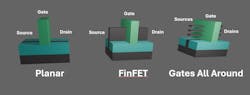
In the semiconductor world, greater density and efficiency are tantamount to device scaling. Conventional scaling through planar complementary metal-oxide semiconductor (CMOS) devices reached physical and leakage limits decades ago. Then came FinFETs, which extended Moore’s Law further by introducing a fin-shaped channel that improved gate control. But FinFETs, too, have reached their limits.
As gate lengths approach single-digit nanometers, electrostatic short-channel effects and leakage once again constrain scaling. Simply put, FinFETs can’t provide the level of gate control needed for sub-3-nm logic.
Now, the industry is turning to gate-all-around (GAA) transistors as the next path forward. By surrounding the channel with gate material on every side, GAA devices minimize leakage and variability even at angstrom-level dimensions.
Gate-All-Around Structure and Advantages
A GAA transistor is fabricated by vertically stacking thin silicon channels separated by sacrificial silicon-germanium (SiGe) layers. Once the SiGe is selectively etched away, the remaining nanosheets are completely wrapped by the gate dielectric and gate metal.
By fully surrounding the gate at every angle, the architecture is essentially the logical conclusion of the electrostatics journey that began with planar devices, was extended by FinFETs, and now reaches full surround-gate control.
The first, and most important, benefit of GAA is that the unique geometry enables far tighter control of the channel potential. Drain-induced barrier lowering and other short-channel effects, which become crippling as devices scale, are suppressed because the gate exerts influence from all sides. At the same time, the ability to stack multiple nanosheets vertically allows designers to increase drive current without consuming more horizontal area.
Together, these features provide the power, performance, area, and cost (PPAC) benefits that FinFETs can no longer sustain.
Of course, these gains come at the expense of fabrication complexity. Each nanosheet stack requires multiple epitaxial growth steps, precision etching of sacrificial layers, and integration of high-k dielectrics and metal gates into ever-thinner vertical spaces. The structural advantages of GAA are therefore only part of the story. The new geometry also redefines where the performance bottlenecks appear.
Why GAA Faces New Challenges
Although GAA devices solve the electrostatics problem, they introduce a different limitation. In planar devices, the channel resistance was dominant. In FinFETs, resistance from the source and drain became comparable to the channel contribution. With GAA, contact and source-drain resistance now account for most of the total resistance, effectively capping how much current can be driven at a given supply voltage.
This shift is the result of multiple converging factors. The source and drain must be doped to extraordinarily high levels to minimize series resistance, sometimes approaching the atomic density of silicon itself.
These heavily doped regions lie directly adjacent to the undoped nanosheet channel, which is incredibly sensitive to even minimal dopant diffusion. A handful of phosphorus or boron atoms drifting into the channel can alter threshold voltage, increase leakage, and introduce variability across stacked nanosheets.
At the same time, the process of removing sacrificial SiGe layers to free the nanosheets risks leaving rough silicon interfaces. That roughness scatters carriers, degrades mobility, and further limits current drive. Finally, the last step of forming metal contacts introduces an additional resistance penalty through the Schottky barrier at the interface.
The net result is that GAA transistors, though superior in electrostatics, are constrained by a different bottleneck. Where AI and embedded workloads depend on both high performance and low energy per operation, this imbalance presents a serious challenge.
MST: Atomic-Scale Engineering for GAA
One promising solution to these challenges is Atomera’s Mears Silicon Technology (MST). MST introduces ultra-thin epitaxial layers of silicon with partial monolayers of oxygen at specific points in the device structure to control dopant diffusion, smooth channel interfaces, and reduce resistance.
Importantly, MST isn’t a wholesale redesign of the transistor, but an insertion that leverages existing epitaxial steps in the process flow. As a result, MST fits nicely with GAA fabrication, which already requires multiple epitaxy stages.
The most direct role for MST in GAA fabrication is as a diffusion barrier between heavily doped source-drain regions and undoped channels. Because the channel must remain clean of dopants to switch predictably, any migration from the source-drain compromises performance.
MST layers sharply reduce this diffusion so that manufacturers can drive activated dopant levels higher in the source-drain to cut resistance without contaminating the channel. Experimental results show that this barrier effect can reduce off-state leakage by orders of magnitude while preserving threshold uniformity.
MST also improves mobility in the channel. At the high vertical electric fields that are typical of nanosheet logic devices, scattering from surface roughness becomes the dominant mobility limiter. Because it improves the interface quality, MST reduces roughness scattering and increases mobility by around 15% under standard operating conditions. Such an improvement directly translates into higher drive current at the same supply voltage and faster switching without proportional increases in power.
Another identified benefit is the ability of MST to alter the effective work function of the gate stack. Traditional GAA devices require thick work-function metals for low-threshold devices that limit vertical stacking density. MST reduces the interfacial dipole at the silicon/high-k boundary to lower threshold voltage without thick metals.
This change allows more nanosheets to be packed within the same vertical space, thereby increasing the drive current per footprint by roughly 10%.
Finally, MST lowers contact resistance by reducing the Schottky barrier height between metal and silicon. Studies show reductions of more than 40% in barrier height, corresponding to an 11% decrease in overall contact resistance. Since contacts have become the dominant contributor to device resistance in GAA, even modest reductions translate into significant performance improvements.
Implications from Hyperscale to the Edge
The pressures on compute efficiency extend from the largest cloud data centers down to the smallest edge devices, and both face the same PPAC tradeoffs.
At hyperscale, training and running large AI models require enormous compute density. Yet growing energy consumption and cooling demands threaten sustainability. Any reduction in leakage current or contact resistance translates directly into megawatts of savings across racks of servers (i.e., the power side of PPAC).
MST-enabled GAA devices raise performance by improving carrier mobility and lowering resistance, which increases drive current per transistor. By unlocking thinner work-function metals and denser nanosheet stacking, MST improves transistor area efficiency to maximize throughput per square millimeter of silicon. Together, these factors lower the cost per operation at scale by reducing energy overhead and infrastructure requirements.
The same advances that optimize PPAC at hyperscale also apply to embedded and edge systems, which operate under the opposite set of constraints. Instead of megawatt budgets, edge designers manage milliwatts in small form factors with limited cooling capacity. Yet these devices must now deliver sophisticated AI inference and real-time control.
MST’s diffusion blocking keeps threshold voltages stable to improve yield and reliability across billions of transistors. Lower contact resistance and higher mobility translate into more operations per watt, directly addressing power constraints. Improved stacking density reduces silicon footprint to address area and cost while offering higher levels of integration. For edge engineers, the results are compact processors that achieve higher performance without exceeding thermal or energy limits.
Conclusion
As the industry advances into the angstrom era, gate-all-around architectures combined with atomic-scale materials engineering provide a sustainable path forward. The demands of AI and edge computing are immense, but with GAA and innovations such as MST, the semiconductor industry has the tools to meet them.
About the Author
Robert Mears
Chief Technology Officer and Founder, Atomera
Dr. Robert Mears is a recognized pioneer and leading expert in photonics and nanoscale material engineering with more than 30 years’ experience. Dr. Mears has authored or co-authored approximately 250 publications and patents and is an Emeritus Fellow of Pembroke College, Cambridge, England.
Comment About the Article
To join the conversation, and become an exclusive member of Electronic Design, create an account today!

Leaders relevant to this article: