Designing with Rad-Hard Bare-Die Power and Memory Semiconductors
What you’ll learn:
- How bare-die semiconductors significantly reduce size and weight.
- How custom packaging and direct thermal management improve heat dissipation and environmental resilience.
- Using bare die can accelerate development cycles by providing earlier access to radiation-hardened components.
In the rapidly evolving fields of aerospace, defense, and space applications, the demand for high-performance, reliable electronics that can withstand harsh environments is greater than ever. Among the critical choices faced by system designers is the selection between radiation-hardened (rad-hard) bare-die semiconductors and their prepackaged counterparts, particularly for power-management and memory functions.
This article explores the advantages and benefits of using radiation-hardened bare-die power and memory semiconductors, in comparison to traditional prepackaged semiconductors.
Understanding Radiation-Hardened Semiconductors
Radiation-hardened semiconductors are engineered to resist the damaging effects of ionizing radiation, such as cosmic rays, solar flares, and nuclear events. These effects, including total ionizing dose (TID), single event effects (SEE), and displacement damage, can cause malfunction, data corruption, or permanent failure in electronic devices. Applications in space, defense, and nuclear environments demand such robust solutions to ensure mission-critical reliability and success.
These semiconductors come in two primary forms:
- Bare die: The semiconductor chip is supplied without an encapsulating package, enabling easier integration into customer-specific power and/or memory multichip modules (MCMs).
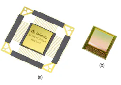
- Prepackaged: The semiconductor chip is enclosed in a standard package (e.g., plastic or ceramic hermetic) with external leads, ready for standard board-level mounting (Fig. 1).
Key Advantages of Radiation-Hardened Bare-Die Semiconductors
There are numerous reasons for designers to opt for bare die over packaged parts:
1. Size and weight reduction
Bare-die semiconductors offer significant advantages in size and weight. By eliminating the external package, the physical footprint of the component is drastically reduced. This is crucial in applications where space and weight are at a premium, such as satellites, spacecraft, and advanced defense systems.
The reduction in both size and weight translates to more compact system designs, increased payload capacity, and lower launch costs for space missions.
2. Enhanced design flexibility and integration
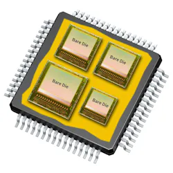
Bare-die components allow system designers to create highly integrated MCMs and system-in-package (SiP) solutions (Fig. 2). Designers can combine power, memory, logic, and other functions into a single hybrid circuit, tailored to specific application needs. This level of advanced integration is difficult to achieve with prepackaged parts due to package incompatibilities, increased parasitic effects, and the physical limitations of standard packages.
3. Superior electrical performance
Direct access to the die allows for shorter interconnections and minimized parasitic inductance and capacitance. This results in:
- Faster switching speeds
- Lower signal propagation delays
- Reduced power losses (i.e., higher efficiency)
- Improved signal integrity
Such performance enhancements are particularly valuable in high-speed memory and power-management applications, where prepackaged components might introduce unwanted electrical artifacts due to their internal leads and bond wires.
>>Download the PDF of this article, and check out the TechXchange for similarly themed articles and videos

4. Customization and application-specific packaging
With bare die, customers can dictate the packaging technology, materials, and layout that best suit their operational environment and application requirements. Whether it’s hermetic sealing, advanced thermal management, or unique form factors, bare-die components can be incorporated into custom packages or directly mounted onto substrates using chip-on-board (COB) or flip-chip techniques. This flexibility is typically unavailable with prepackaged semiconductors, which are limited to standard industry packages.
5. Improved thermal management
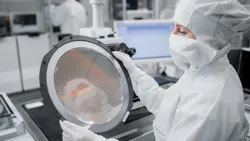
Heat dissipation is a critical challenge in high-power and high-reliability systems. Bare-die assemblies often allow for more efficient thermal paths, as the die can be mounted directly onto heatsinks or thermal substrates (Fig. 3).
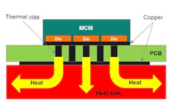
This direct thermal interface can dramatically improve heat dissipation compared to prepackaged devices, where the package itself may act as a thermal bottleneck. Enhanced thermal management leads to greater power-handling capability and longer device life.
6. Increased radiation tolerance
While both bare die and prepackaged parts can be fabricated with radiation-hardened processes, bare-die usage will further enhance system-level radiation tolerance. Custom packaging or direct die attachment makes it possible to use radiation-shielding materials or configurations that provide superior protection compared to standard packages. In addition, bare die can be strategically placed within the system to minimize exposure to radiation-intensive regions.
7. Supply chain and lead-time advantages
In many cases, rad-hard bare-die semiconductors are available earlier in the product development cycle than their prepackaged equivalents. That’s because the packaging development, qualification, and testing phases can add significant time to the availability of prepackaged parts. For projects on tight schedules, leveraging bare die typically accelerates prototyping and system integration.
Comparison to Prepackaged Semiconductors
Prepackaged radiation-hardened semiconductors offer ease of handling, standardized interfaces, and off-the-shelf availability. They’re ideal for applications where:
- Standardization is critical
- System requirements are less stringent
- Rapid prototyping is needed
However, when compared to bare die, prepackaged parts often fall short in areas where custom integration, performance, and environmental resilience are paramount. Some of the key limitations include:
- Larger size and weight due to packaging
- Increased electrical parasitics
- Limited thermal-dissipation paths
- Inflexibility in custom module design
Specific Applications Where Bare Die Can Make a Significant Impact
Spacecraft and Satellites
Space missions demand ultra-reliable electronics that are lightweight, compact, and capable of withstanding extreme radiation. Bare-die components are preferred for building hybrid microcircuits that pack maximum functionality into the smallest possible volume, with tailored shielding and thermal solutions.
Defense Systems
Ruggedized electronics for missile defense systems, avionics, and secure communications benefit from the integration, performance, and reliability offered by bare die semiconductors. Custom packaging enables compliance with stringent military standards for shock, vibration, and radiation exposure.
Medical Devices and Nuclear Instrumentation
In environments with high radiation exposure, such as nuclear reactors or cancer therapy equipment, bare-die solutions allow for custom, radiation-shielded assemblies that ensure patient safety and equipment longevity.
Challenges and Considerations of Bare-Die Use
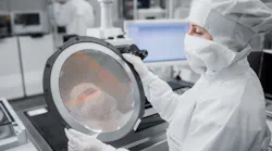
While the advantages of bare-die semiconductors are significant, their use does come with specific challenges. That’s why it’s critical for designers and system integrators to work with established and trusted semiconductor companies like Infineon IR HiRel (IR HiRel). Such firms have the in-house expertise, experience and manufacturing capabilities to manufacture, test, supply, and handle best-in-class bare-die products (Fig. 4).
Nonetheless, for mission-critical systems where performance and reliability are non-negotiable, these challenges are typically outweighed by the benefits.
Industry Trends and the Future of Bare Die in Rad-Hard Apps
The drive toward miniaturization, higher performance, and increased integration is accelerating the adoption of bare-die solutions in radiation-sensitive environments. Advances in die-level interconnect technologies, such as through-silicon vias (TSVs), wafer-level packaging (WLP), and advanced flip-chip assembly, are making bare-die integration more accessible and robust than ever before.
As the commercial space industry grows and government agencies continue to push the boundaries of exploration and defense, the demand for flexible, high-reliability, radiation-hardened electronics will only increase. Bare-die power and memory semiconductors will play a pivotal role in enabling these next-generation systems.
Conclusion
Radiation-hardened bare die power and memory semiconductors offer a compelling array of advantages over prepackaged alternatives, ranging from size and weight reduction to superior performance, integration, and customization. While the use of bare die requires specialized handling and design expertise, the benefits for mission-critical, high-reliability applications are considerable.
For system designers facing the unique challenges of space, defense, and high-radiation industrial environments, the adoption of radiation-hardened bare-die semiconductors is often the key to achieving the highest levels of performance, reliability, and innovation.
Infineon's IR HiRel is in a unique position in the industry to offer many of its products in bare-die form. Depending on the application and quantities, IR HiRel can work with customers to convert most parts to bare die if they don’t already exist in the company’s standard product portfolio.
>>Download the PDF of this article, and check out the TechXchange for similarly themed articles and videos
About the Author

Joseph Dussi
Senior Digital Marketing Manager, Infineon Technologies
Joe Dussi combines technical and marketing expertise. He holds a mechanical engineering degree. He spent over a decade designing advanced propulsion systems for U.S. Navy surface and subsurface vessels, as well as contributing to key defense initiatives. In the semiconductor industry, he has 25+ years of marketing experience with Analog Devices (ADI), Qorvo, and now Infineon IR HiRel. His diverse background bridges engineering innovation and market strategy.
Comment About the Article
To join the conversation, and become an exclusive member of Electronic Design, create an account today!

Leaders relevant to this article: