Chiplets: Making the Pieces Work Together
What you’ll learn:
- Why chiplet performance is increasingly limited by end-to-end communication, not just packaging density.
- How latency and bandwidth scale (and sometimes break) as you add chiplets, hops, and protocols.
- Why coherence is the “hidden tax” in shared-memory chiplet systems, and how standards like CXL and UCIe shape the design space.

If you ask most engineers what makes chiplets hard, the first answer is usually packaging: interposers vs. organic substrates, thermal paths, bump pitch, signal integrity, yield, and assembly. Those topics matter, but they’re no longer the full story.
The deeper shift is architectural. Chiplets turn a “single-die computer” into a distributed system in a package. And as distributed systems have taught us for decades, performance is rarely limited by raw compute alone. It’s limited by communication: the latency of moving data, the availability of bandwidth, and the cost of maintaining a consistent view of memory across many participants (see USENIX’s chiplet network scaling paper).
Packaging Enables Chiplets — Interconnect Determines Whether They Behave Like One System
Chiplets exist because the industry needs new ways to scale beyond the practical limits of monolithic dies — reticle limits, yield constraints, and the desire to mix process nodes and functions. Modern die-to-die standards reflect that motivation explicitly. The UCIe Consortium describes UCIe as a package-level die-to-die interconnect standard that spans physical layer, protocols, and software/compliance, aiming to make multi-vendor chiplet composition feasible (see UCIe Consortium’s specifications).
That “full-stack” framing is important. You can assemble chiplets into a package and still fail to build a coherent system if the communication stack is poorly matched to the workload.
A practical way to think about the stack is:
- Physical connectivity: Bumps, bridges, interposers, or hybrid bonding determine wiring density and reach.
- Link/adapter behavior: Training, flow control, CRC/retry, lane repair, and clock-domain crossings determine reliability and latency variability.
- Protocol semantics: Streaming I/O isn’t the same as cache-coherent shared memory.
- System fabric behavior: Topology, routing, and congestion control determine whether “peak bandwidth” translates into application throughput (see Open Compute Project’s BoW interface specs).
Latency: Chiplets Introduce Hops, Boundaries, and Extra Round Trips
In a monolithic SoC, many data paths are short, and architects can often hide latency behind locality (caches) and high-frequency interconnects. Chiplets change that because even “nearby” resources may now sit behind a die-to-die boundary.
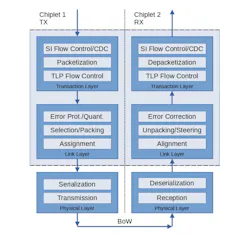
At the link layer, die-to-die stacks commonly require packetization, alignment, and clock-domain crossing between the die-to-die interface and the on-die interconnect clock domain functions called out explicitly in the Open Compute Project’s Bunch of Wires (BoW) link-layer specification (See UCIe Consortium's 3.0 specification announcement). Each stage can add latency, and multi-hop topologies compound it.
At the system level, large-scale chiplet networks can replace a few large switches with many smaller hops (Fig. 1). That can be attractive economically, but it increases network diameter and makes hop-by-hop behavior critical. In shared-memory systems, it becomes even more sensitive because hardware coherence can be extremely demanding on the network.
The key takeaway for designers is that “die-to-die latency” isn’t one number. It’s the sum of PHY/link overhead, buffering, routing, and (often) coherence-induced round trips.
On-Package links are Fast, But Bandwidth Efficiency is the Real Battle
The industry is pushing more communication into the package because on-package links can be dramatically denser and more energy-efficient than board-level I/O. Recent UCIe public releases illustrate this trajectory:
- UCIe 2.0 highlights support for 3D packaging (UCIe-3D) to enhance bandwidth density and power efficiency, with hybrid-bonding-friendly pitch ranges down toward ~1 µm.
- UCIe 3.0 highlights higher signaling rates (48/64 GT/s) and extended sideband reach to enable more flexible multichip configurations.
At the same time, alternative die-to-die stacks like BoW emphasize scalable frameworks and layered architectures designed to map higher-level protocols onto efficient electrical interfaces.
But the real engineering challenge is that bandwidth is easy to allocate on a diagram and hard to deliver under contention. As you add chiplets, two effects tend to show up:
- First, traffic becomes burstier and more heterogeneous (compute-to-memory, accelerator-to-memory, chiplet-to-chiplet collectives, etc.), so congestion and backpressure begin to dominate tail latency (Fig. 2). Large-scale chiplet network work stresses that fine-grained simulation is needed because these effects are structurally tied to hop-by-hop behavior.
- Second, planar designs can become constrained by how many signals are able to reach the die edge (“shoreline”), encouraging 3D approaches or more careful partitioning of what must be “near” vs “far” (see SemiEngineering’s UCIe Technical Components).
Coherence: The “Hidden Tax” that Turns Bandwidth into Performance
If latency and congestion are the visible problems, coherence is the hidden one because it turns ordinary loads/stores into network events.
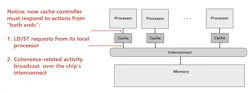
The reason is fundamental: To maintain correctness, coherence protocols must ensure that all participants see a consistent view of shared data. In snooping-based protocols, that may require every cache (or agent) to observe coherence traffic, adding interconnect load that scales poorly as the number of participants grows (see Carnegie Mellon University’s cache-coherence lecture).
Directory-based protocols reduce broadcast pressure with point-to-point messaging and explicit state. However, they can introduce extra indirections and multi-hop sequences that increase latency (see University of California, Berkeley’s memory systems lecture).
Chiplets intensify this tradeoff. A coherence miss that used to be a short on-die event can become a multi-hop, multi-die round trip (Fig. 3). And that could happen at extremely high rates in AI and data-center workloads where many compute engines share memory or share cached working sets.
This is where coherence-capable standards and ecosystems matter. Electronic Design’s own technical coverage describes Compute Express Link Consortium’s CXL as a cache-coherent interconnect that multiplexes I/O, caching, and memory semantics, maintaining a unified coherent memory space between host and attached devices. Public CXL 3.1 materials emphasize fabric extensions and manageability improvements aimed at scaling disaggregated systems, reflecting how coherence is increasingly treated as a system fabric capability rather than a point link feature (see Compute Express Link Consortium’s CXL 3.1 specification).
UCIe’s public positioning aligns with this direction: It explicitly references leveraging PCIe and CXL as part of the die-to-die approach, enabling “coherent semantics in-package” when the architecture needs it.
The Next Scaling Frontier: DFx, Manageability, and Predictable Behavior
As chiplets scale, system developers face another reality: You can’t debug a multichip package the way you debug a typical board-level design.
UCIe 2.0’s public release emphasizes DFx (testability, debug, telemetry, manageability) across the system-in-package lifecycle, including standardized approaches so that multi-vendor chiplets can be managed coherently. Presentations tied to UCIe 2.0 also note practical constraints such as limited probe access with microbumps, motivating holistic management fabrics and remote access mechanisms.
Packaging roadmaps reinforce why this matters. Technology briefs from Intel on EMIB and 3D stacking discuss pitch regimes and integration approaches that increase density, and therefore increase the need for robust monitoring and predictable link behavior as signal margins shrink.
Independent industry briefs similarly argue that hybrid bonding is essential beyond microbump scaling limits to drive lower energy per bit and higher bandwidth density, which again increases the importance of run-time calibration, error detection, and repair mechanisms (see Applied Materials Hybrid Bonding Scaling).
One subtle but important design lesson: If interconnect is now a first-class system resource, it needs first-class instrumentation. The job isn’t only to hit a peak GT/s target; it’s to deliver predictable latency and sustained bandwidth under real workload contention, across PVT variation, over lifetime.
Design Takeaways for Engineers Building Chiplet-scale Systems
The chiplet era is forcing a mindset change — you architect the communication first, then place compute around it. In practice, this means:
- Don’t treat die-to-die links as “big wires.” Treat them as a network with congestion, traffic classes, and failure modes.
- Decide early which interactions must be coherent shared memory and those that can be message/DMA style because coherence will shape topology, buffering, and ordering constraints.
- Evaluate scaling via architecture exploration and modeling, not just peak-link specs; chiplet surveys emphasize that EDA/automation and correct partitioning are central to realizing chiplet benefits (See arXiv’s chiplet/system architecture research).
- Plan for DFx and manageability as part of the interconnect stack, especially as bump pitches shrink and direct probing becomes impractical (See UCIe Consortium’s Architecture and Ecosystem Overview).
Conclusion
Chiplets are often introduced as a packaging solution to economic and scaling limits. But at system scale, the defining problem is no longer “Can I connect these dies?” It’s “Can I make them behave like a single computer under real workloads?”
That’s why interconnect (latency, bandwidth efficiency, and coherence) has become the differentiator. The designers who win in the chiplet era will be those who treat the fabric as the system, and engineer communication with the same rigor they apply to compute.
References
- UCIe Consortium’s Specifications.
- Compute Express Link Consortium’s CXL 3.1 Specification.
- SemiEngineering’s UCIe Technical Components.
- USENIX’s Chiplet Network Scaling Paper.
- Carnegie Mellon University’s Cache Coherence Lecture.
- University of California, Berkeley’s Memory System Lecture.
- arXiv’s Chiplet/System Architecture Research.
- Open Compute Project’s BoW Interface Spec.
- Intel’s EMIB Product Brief.
- Applied Materials’ Hybrid Bonding Scaling.
- UCIe Consortium’s 3.0 Specification Announcement.
- UCIe Consortium’s Architecture and Ecosystem Overview.
>>Check out the TechXchange for similarly themed articles and videos

About the Author

Kent Orthner
Principal Solutions Architect, Baya Systems
Kent Orthner has over 25 years of experience designing all aspects of on-chip networks, FPGA technology, and high-speed silicon connectivity. Before joining Baya Systems, Kent served as Sr. VP of Engineering at Achronix Semiconductor, where he led the development of cutting-edge FPGA devices and IP solutions, including the FPGA-embedded high performance on-chip network. Before Achronix, Kent served as the Vice President of Engineering at Arteris, where he was responsible for all hardware and software development, and where he developed and released the world’s first highly scalable and configurable cache-coherent interconnect IP. Before that, Kent spent 11 years at Altera, leading multiple cross-functional engineering teams, including Altera's NoC design tool suite, IP infrastructure, and debug and design visibility tools. Kent holds a Master of Engineering in Electrical Engineering from Carleton University, Canada, and a Bachelor of Applied Science in Computer Engineering from the University of Ottawa, Canada.
Comment About the Article
To join the conversation, and become an exclusive member of Electronic Design, create an account today!

Leaders relevant to this article: