IBM 7-Angstrom Tech Squeezes in 100 Billion Transistors
What you’ll learn:
- What are the challenges with sub-1-nm transistors?
- What is the 3D nanostack configuration?
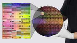
We’re down to counting atoms when it comes to IBM’s latest sub-1-nanometer transistor technology (Fig. 1). This technology will initially target high-end AI data centers that have a need for higher-performance systems. The transistors use a gate-all-around or nanosheet approach.
Smaller transistors usually mean better performance and greater power efficiency. In this case, the new 7-Å devices bump up performance by 50% while improving power utilization by 70% compared to IBM’s 2-nm node.
Designers still have the reticle limit when it comes to production, but making transistors smaller means packing in more within that limit. Packaging technologies like chiplets allow designers to build systems that would not be possible with a single die. Chiplets also make it possible to mix die with different transistor technologies and different functionality like high bandwidth memory (HBM).
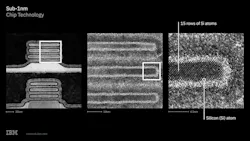
3D die stacking has been common with solutions like HBM. However, this technology layers die atop each other. The nanostack does it at the transistor level albeit with only a few levels (Fig. 2). IBM’s research has projected that a 4-track staggered design will deliver a 50% area improvement while reducing power requirements. Both are designed to increase density.
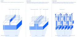
IBM’s nanostack configuration is built on a multichannel, nanosheet-on-nanosheet NanoStack CMOS architecture. It employs a vertical inter-FET isolation.
The company’s announcement is about the technology and possibilities rather than release of production devices, but that will come. In the meantime, these announcements highlight how the next generation of electronic devices will be constructed.
About the Author

William G. Wong
Senior Content Director - Electronic Design and Microwaves & RF
I am Editor of Electronic Design focusing on embedded, software, and systems. As Senior Content Director, I also manage Microwaves & RF and I work with a great team of editors to provide engineers, programmers, developers and technical managers with interesting and useful articles and videos on a regular basis. Check out our free newsletters to see the latest content.
You can send press releases for new products for possible coverage on the website. I am also interested in receiving contributed articles for publishing on our website. Use our template and send to me along with a signed release form.
Check out my blog, AltEmbedded on Electronic Design, as well as his latest articles on this site that are listed below.
You can visit my social media via these links:
- AltEmbedded on Electronic Design
- Bill Wong on Facebook
- @AltEmbedded on Twitter
- Bill Wong on LinkedIn
I earned a Bachelor of Electrical Engineering at the Georgia Institute of Technology and a Masters in Computer Science from Rutgers University. I still do a bit of programming using everything from C and C++ to Rust and Ada/SPARK. I do a bit of PHP programming for Drupal websites. I have posted a few Drupal modules.
I still get a hand on software and electronic hardware. Some of this can be found on our Kit Close-Up video series. You can also see me on many of our TechXchange Talk videos. I am interested in a range of projects from robotics to artificial intelligence.
Comment About the Article
To join the conversation, and become an exclusive member of Electronic Design, create an account today!

Leaders relevant to this article: