Data-Center CPU’s Dual-Chiplet Design is Intent on AI
This article is part of the TechXchange: Chiplets - Electronic Design Automation Insights.
According to Intel, its latest data-center CPU, which packs up to 64 cores spread out over a pair of chiplets bonded together with its 2.5-D EMIB technology, is the best CPU for AI on the market.
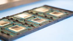
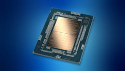
The fifth-generation Xeon Scalable CPU, code-named "Emerald Rapids,” is a giant data-center processor that binds together a pair of 32-core CPU tiles. It thus behaves as a single slab of silicon that features 3X more L3 cache (320 MB) than its predecessor and a faster DDR5 memory controller that ranges up to 5600 MT/s. For faster I/O bandwidth, PCIe Gen 5 and CXL 1.1 connectivity is supported.
Intel’s latest hardware isn’t as large of a technological leap as the current “Sapphire Rapids” CPU rolled out at the start of 2023. And it lacks the process and packaging innovations in the pipeline with “Granite Rapids,” the code-name for its future high-performance Xeon, due out in late 2024.
Still, the semiconductor giant is using Sapphire Rapids as a template for its new dual-chiplet data-center CPU, while ushering in improvements from the CPU to the SoC.
The new Xeon CPU is based on a more polished formulation of the same Intel 7 process node used in Sapphire Rapids. Despite that, it’s designed to deliver average gains in general-purpose performance of about 21% over many of the most widespread workloads in data centers.
Intel is also upgrading the accelerators that are attached directly to the cores to run specific chores, ranging from high-performance computing to networking, storage, and security, faster and more efficiently than the CPU itself. Intel is also baking better AI acceleration into the server CPU with its Advanced Matric Extensions (AMX) and Advanced Vector Extensions (AVX-512) instructions.
“Xeon is the best CPU for AI,” said Lisa Spelman, corporate VP and GM of Intel’s Xeon processors, in a pre-briefing with journalists and analysts at Intel’s office outside Portland, Oregon. “And while AI is important, we’re not losing sight and we’re continuing to invest in delivering leadership performance across every customer workload.”
Intel is under fierce competitive pressure from AMD, specifically in data centers that are packed with thousands of high-end processors that can cost more than $10,000 each, and Nvidia, which is tapping into the boom in AI chips.
But the company is keen to prove that it’s executing on the ambitious roadmap being pursued under CEO Pat Gelsinger. After delaying the Sapphire Rapids CPU several times, Intel executives touted the fact that the company is supplying the new data-center CPU to customers and is ready to ramp up production.
“We’re getting our act back together and delivering products on schedule,” Gelsinger said at the pre-briefing.
Advanced Packaging Plays Its Part for Intel
In Sapphire Rapids, Intel combines four CPU tiles, also referred to as a die or chiplet, into one large processor package with up to 60 cores, marking the first time that it integrated chiplets into its flagship Xeon data-center CPU family.
The major difference with Emerald Rapids is that it integrates a pair of CPU tiles, which helps it recover some of the power efficiency and performance that was surrendered with the shift to a “disaggregated” design in the first place.
This contrasts with AMD, which has long been using a chiplet architecture in its general-purpose data-center CPUs by applying a concept called system-technology-co-optimization (STCO). Unlike Intel’s, the data-center chips from AMD co-package several CPU tiles (also called compute complex dies, or CCDs, in AMD parlance) around separate silicon die split from the CPU and built on a slightly less advanced node that contains I/O and memory controllers.
Intel said Emerald Rapids consists of a pair of chiplets that bring everything required in a 64-bit server CPU to the table, including memory, connectivity, and CPU cores themselves linked via a mesh interconnect. In many ways, they’re full-fledged CPUs. As a result, they’re larger than the compute tiles at the heart of AMD’s Genoa data-center CPU, which is touted as the fastest general-purpose server CPU in the market with up to 96 cores in all.

In Emerald Rapids, Intel said it’s also raising the processing capacity of the CPU, wringing out up to 15% more instructions per clock cycle (IPC) over the “Golden Cove” core at the heart of Sapphire Rapids, as well as increasing the number of cores per package to 64.
These tiles are mirror images of each other and are bound together horizontally using Intel’s 2.5-D advanced packaging tech, called embedded multi-die interconnect bridge (EMIB). EMIB is a thin sliver of silicon that consists of die-to-die interconnects used by the chiplets to chat with each other. These are placed inside the packaging substrate underneath the edges of the tiles, giving them the ability to act as close to a monolithic design as physically possible, said Intel.
Placing everything in a data-center CPU on a monolithic system-on-chip (SoC) has its upsides: the interconnects between cores are faster since they’re on the same plane of silicon and it has a single power interface to manage. But as the world moves to smaller process nodes, having one large slab of silicon does draw some downsides. Larger chips are more prone to defects during manufacturing, which brings down yield and cost, and flexibility is limited.
Instead, the movers and shakers in the semiconductor industry are breaking them apart into a set of smaller chiplets that can be manufactured more affordably and made using the most optimal process technology.
By spreading out transistors over several tiles and binding them together in a large system-in-package (SiP), it can also squeeze in more silicon than what’s possible with a single monolithic SoC. Today, the manufacturing (or reticle) limit of a single SoC is in the 800-mm2 range, which limits the number of transistors that can be placed on it. Using chiplets gives you a way to cram more than 1000 mm2 per package, while preserving the monolithic qualities of the design. Intel has stated that each CPU tile in Sapphire Rapids is roughly 400 mm2, adding up to a total of around 1600 mm2.
But the tradeoff is connectivity and power. The die-to-die interconnects used by the tiles to communicate with each other come with a power and latency penalty that takes a toll on the processor’s performance.
Even though the CPU tiles in Sapphire Rapids act logically as a single monolithic chip, they can cause fluctuations in performance when a workload needs to cross over into other tiles to access more computing power or memory than a single tile can supply, said Intel Senior Fellow Silesh Kottapalli.
However, reducing the number of chiplets in Emerald Rapids and the number of EMIB connections between them means less die-to-die data movement. This ultimately saves several percentage points worth of power and latency, said Intel.
Surrounding the CPU: Faster Memory and Connectivity
The simpler chiplet architecture is coupled with the significantly larger L3 cache for a “double uplift” in performance, said Kottapalli. Having up to 320 MB of memory (up from the 112.5 MB of shared cache in Sapphire Rapids) placed close to the CPU helps keep the cores from falling behind on high-performance computing (HPC), AI, and other heavy-duty workloads, the company said.

Despite the larger L3 cache, the chip lacks the same amount of memory as AMD’s V-Cache technology, a cache-memory chiplet that’s stacked directly on top of AMD’s highest-end CPU cores, including in its Genoa server CPU.
Intel increased the memory frequency in the CPU’s memory controllers, supporting up to eight channels of DDR5 DRAM as fast as 5600 MT/s, up from 4800 MT/s in Sapphire Rapids. Since memory capacity and bandwidth are bottlenecks in AI, the additional on-chip memory and faster I/O and memory controllers are a boon there, said Intel.
To facilitate fast connectivity to accelerators and memory in the system, the CPU is equipped with PCIe Gen 5 lanes. The lanes can also be configured for Compute Express Link (CXL) 1.1, a cache-coherent interconnect that’s on the verge of taking over the data center. CXL primarily focuses on attaching the CPU to additional memory using its spare PCIe lanes.
The CPU supports up to four channels of CXL memory. These can act as separate tiers of memory by software or as a single tier of 12-channel DRAM for the purposes of capacity or bandwidth expansion.
While its latest Xeon CPU is in the same power envelope (up to 350 W) as its predecessors, a raft of power-saving enhancements in the CPU and the SoC itself gives it up to 36% better performance per watt at the package level.
Intel also further enhanced the “Optimized Power Mode” that was introduced in Sapphire Rapids. It ups the power efficiency when the CPU isn’t running at full power and when it’s idle (at a load of 0%).
What’s Inside a CPU Designed for AI?
Intel is also striving to show its progress in running machine learning directly on its CPUs.
The company said it made several key improvements to AMX, the primary AI accelerator in its data center CPUs. Introduced in Sapphire Rapids, the accelerator is specifically designed to run matrix multiplication, a class of operations widely used in AI inferencing, including for large language models (LLMs). AMX is also closely related to Intel's AVX-512 instruction, which is also relevant for AI.
These accelerators aren’t separate cores in the sense of a neural processing unit (NPU), which Intel is plugging into its Meteor Lake chip for PCs. They are instructions that exist within the CPU.
Intel said the next-gen CPU can more carefully direct power to the AMX and AVX-512 accelerators inside, reducing the performance hit that can happen when these instructions are engaged. As a result, it wrings out faster clock frequencies from the CPU when it's carrying out AI workloads. Better power delivery along with the architectural improvements throughout the CPU adds up to 42% faster AI inferencing in some cases, Intel said.
AMX adds the ability to run AI workloads using truncated 8-bit numbers, called INT8, that are used for inferencing when the precision of FP32, a single-precision floating-point format used for AI, isn’t required. Because it has less precision, more AI operations can be processed per cycle. The accelerator can also run 16-bit data called BF16, an attribute that speeds up training and inferencing of some facets of the largest transformer-based neural networks.
There are other applications for the AI accelerators in its hardware. According to the company, it’s possible to use AMX and AVX-512 in tandem to implement a scheme called “sparsity.” It removes everything irrelevant from the neural network so that the CPU can run the smaller model faster while consuming less power overall.
So, instead of buying new silicon, customers can reuse what they have already deployed in their data centers. “It’s not one size fits all,” said Sandra Rivera, executive VP and GM of Intel’s Data Center and AI Group, in reference to AI silicon.
While the CPU is the backbone of the data center, the largest and most capable AI models, including OpenAI's GPT-4, Google’s Gemini, and Meta's Llama largely run on NVIDIA GPUs or other dedicated AI hardware. These chips are frequently packaged with or attached to high-bandwidth memory (HBM) to handle high-end AI models that tend to have more than 100 billion parameters each—a metric that corresponds to their accuracy and complexity. GPUs are typically deployed with CPUs in a 4 to 1 ratio for training or inferencing.
With AI acceleration in every core, Intel said its latest Xeon CPUs have enough power behind them to run smaller AI models toting tens of billions of parameters before attaching a separate accelerator. One advantage to carrying out AI inside the CPU itself is its exclusive high-bandwidth access to on-chip and off-chip memory. Since the CPU is not coordinating with the GPU or other AI accelerator in the system, it also reduces latency, which is one of the most important metrics in AI inference.
While the LLMs behind Microsoft's CoPilot, Google's Bard, and other AI-powered chatbots are huge, they're outliers. Intel noted that the majority of the market is working with smaller AI models that bundle up to 20 billion parameters. The company said its next-gen Xeon CPU can run models in this weight class with less than 100-ms of latency, which it cited as the upper limit for its customers.
Andres Rodriguez, Intel’s chief AI architect, said customers can run even larger LLMs, including Meta’s Llama 2 model with 70 billion parameters and a 40 billion parameter model called Falcon, by spreading them out over four Xeon Scalable CPUs.
Nevertheless, it makes sense to move to a dedicated AI accelerator such as NVIDIA's Hopper GPU or Intel’s Habana Gaudi once you start training or running the largest and most advanced AI models. Intel cites 75 billion parameters or so as the crossover point.
More broadly, Intel is keen to keep investing in software to bring the best out of the CPU, said Spelman.
Read more articles in the TechXchange: Chiplets - Electronic Design Automation Insights.
About the Author

James Morra
Senior Editor
James Morra is the senior editor for Electronic Design, covering the semiconductor industry and new technology trends, with a focus on power electronics and power management. He also reports on the business behind electrical engineering, including the electronics supply chain. He joined Electronic Design in 2015 and is based in Chicago, Illinois.
Comment About the Article
To join the conversation, and become an exclusive member of Electronic Design, create an account today!

Leaders relevant to this article: