Guiding Light: How to Optimize Silicon Photonics with Mixed-Signal Simulation

What you’ll learn:
- How silicon photonics enhances high-bandwidth data movement in modern systems.
- Why advanced simulation techniques are key for designing mixed-signal photonic systems.
- How EDA tools support seamless integration of electrical and optical components.
- Why real number modeling (RNM) improves simulation speed and accuracy.
Today’s computing and communications applications demand unprecedented processing power and high-bandwidth memory access. Data traveling at the speed of light is shaping up to be the solution.
In data centers, GPUs often transfer terabytes of data per second between one another during AI training and inferencing, far exceeding the limits of traditional copper-based interconnects that max out at hundreds of megabits per second. Optical interconnects have emerged as a solution to meet these demands, slinging data at speeds of up to 100 Gb/s using beams of light. But designing and verifying such complex systems requires advanced simulation tools to model their performance and ensure seamless integration of components.
The future of optical connectivity is all about silicon photonics. The tech merges optical and electronic components in a single silicon chip, enabling efficient and high-bandwidth data movement. It’s become more prevalent in areas such as data center interconnects, 5G wireless networks, metro and long-haul telecom, high-performance computing (HPC), and AI. It also has the potential to play a role in quantum computing.
Today, these systems contain a complicated web of analog and digital components. But integrating silicon photonics into these mixed-signal systems adds even more complexity for chip designers and systems engineers. The ability to perform accurate simulations of electrical, optical, and digital domains is vital for developing the high-bandwidth, low-latency connectivity required by AI workloads and other applications.
The Building Blocks of Silicon Photonics
Fundamentally, silicon photonics is all about bringing the speed of light to the world of CMOS.
By integrating components such as lasers, waveguides, and photodetectors onto a single substrate, these systems can precisely manipulate light. The light sources such as lasers and light-emitting diodes (LEDs) encode electrical signals into visible or infrared light, transforming electrons into photons. In contrast, photodiodes and other light detectors perform the reverse process, translating the transmitted light into electrical signals.
The optical waveguides act as conduits for light, analogous to how copper wires convey electrical signals. While the lasers are manufactured separately before being integrated into the system, the waveguide tends to be placed directly on the silicon die. In many cases, these waveguides can be electrically controlled, enabling dynamic control of their refractive index to adjust the phase and intensity of the transmitted light. As a result, these components can be used to filter or modulate the beams of light.
>>Download the PDF of this article, and check out the TechXchange for similar articles


Optical combiners and splitters further enhance system capabilities. Combiners merge signals from multiple sources, allowing for interference-based modulation, while splitters divide optical signals into several different outputs with proportional power distribution. These components form the building blocks of silicon photonics and are essential for applications such as wavelength-division multiplexing (WDM) in data centers.
Silicon Photonics: From Inside the Server to Inside the SoC
Silicon-photonics systems are deployed in various configurations, from standalone devices mounted on PCI Express (PCIe) cards or directly on motherboards to entire racks of servers connected by optical backplanes.
But one of the latest innovations is the integration of optical chiplets in multi-die systems. The systems-on-chip (SoCs) at the heart of these packages are predominantly digital, often containing tens of billions of transistors. These act as the main processing unit for the server or networking switch, communicating with other chips in the system—or, in the case of a switch, the ports for pluggable optics—using electrical I/Os. However, semiconductor firms aim to integrate silicon-photonic transceiver chiplets within the same package to overcome the limitations of electrical I/O.
In the domain of chiplet-based optical interconnects, Intel recently introduced a new OCI-compatible optical chiplet offering 64 bidirectional channels and up to 4 Tb/s of throughput over single-mode fiber. IBM’s co-packaged optics module integrates directly with the host chip, increasing beachfront fiber density sixfold.
The silicon photonics chiplets operate as high-speed optical transceivers. They move data between chips in the same server, in the same rack, and even in different racks over optical fibers instead of copper wires. These architectures illustrate the growing need for accurate simulation of heterogeneous systems that combine analog, digital, and optical domains.
The challenge with co-packaged optics is that silicon-photonics chiplets integrate optical and electronic components, creating complex mixed-signal systems that require rigorous simulation and verification to ensure optimal performance. In addition, chip designers and systems engineers must account for a wide range of other factors, ranging from heat dissipation and power efficiency to signal (SI) and power integrity (PI).
These architectures require a shift in how system-level interactions are modeled and verified. As optics move closer to processing cores, logic simulation must evolve to capture the electrical-optical interactions across diverse timescales and abstraction levels.
For instance, the integration of optical interconnects with RF front-ends—as is the case in the latest heterogeneous silicon-photonic receiver designs—underlines the need for accurate behavioral and layout-aware modeling. A summary of heterogeneous photonic ICs further emphasizes the role of co-simulation across optical, analog, and digital domains.
These developments reinforce the importance of scalable mixed-signal simulation and modeling frameworks that can bridge functionality, physical implementation, and system performance.
The Challenges of Simulating Multi-Die Silicon-Photonics Systems
Nevertheless, designing multi-die systems with integrated silicon-photonic elements presents unique challenges.
Semiconductor vendors often provide process development kits (PDKs) with accurate models of the electronic and optical components for the specific process node supporting silicon photonics. In most cases, these models come in a strictly analog format, such as SPICE or FastSPICE, or in a hardware description language (HDL), such as Verilog-A, Verilog-AMS, or VHDL-AMS, all of which can be used for analog simulations. These models give you high accuracy and relatively fast performance in the analog domain.
However, using analog simulation tools for mixed-signal verification—also called analog mixed-signal (AMS)—can result in prohibitively slow and resource-intensive simulations. These challenges are compounded by the complexity of photonic systems, requiring new approaches to ensure accuracy and efficiency.
Even in relatively simple implementations, the design and verification process can be intricate. For example, a transmitter chiplet using several different light sources at different wavelengths must ensure the receiver chiplet on the other end of the optical fiber can accurately separate and process these signals. The system must verify that optical waveguides and modulators operate effectively under various voltage conditions. The complexity rises significantly when the chiplets are designed to act as transceivers.
Real Number Modeling: The Next Stage in Mixed-Signal Simulation
Real number modeling (RNM) is one way to bridge the gap between the analog and digital domains (see figure).
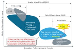
These models enable engineers to simulate analog behaviors using digital tools, significantly enhancing simulation speed and capacity. The most important point is that these models are based on SystemVerilog. As a result, the RNM models can be used to verify and validate analog, digital, and optical components within a unified simulation environment.
By simplifying the simulation process, RNM helps engineers validate intricate mixed-signal systems with increased speed and reliability.
RNM is particularly valuable when analog models created in SPICE or Verilog-A are insufficient for mixed-signal simulations that require integrating photonic elements, analog circuitry, and digital controllers. By enabling high-speed simulation within digital verification workflows, RNMs help eliminate the bottlenecks associated with traditional analog and digital mixed-signal co-simulation.
The Evolving Role of EDA in Silicon Photonics
EDA companies have been rolling out a new class of digital mixed-signal (DMS) simulation tools to help cut through the complexity of integrating optics and electronics.
For instance, the Cadence Xcelium digital simulator fully supports RNM, enabling mixed-signal simulations that integrate photonic and electrical domains. What sets it apart is the speed—the DMS simulation runs significantly faster than traditional AMS simulations. At the same time, it maintains the capacity to model an entire multi-die system.
Cadence also developed a library called PhotoNet, giving engineers access to parameterized RNMs encompassing the most common silicon-photonic components, such as lasers, detectors, waveguides, combiners, and splitters. The new library can be leveraged with the company’s EENet library, which contains parameterized RNM models, representing resistor, inductor, and capacitor devices, along with diodes, transistors, op amps, and other analog functions.
Using PhotoNet, engineers can simulate the functionality of silicon photonics and validate its integration with digital controllers and analog components. PhotoNet models allow engineers to verify that optical waveguides and modulators operate as expected under specific voltage conditions. Coupled with EENet, this approach can verify mixed-signal multi-die systems more efficiently, reducing design iterations and accelerating time-to-market.
Cadence also rolled out Rapid Adoption Kits (RAKs) that provide reference code to show engineers how to model electrical, optical, and digital components in the same system, and then verify that everything works together.
These tools play a critical role in overcoming the challenges of designing and verifying multi-die systems incorporating silicon-photonic components. DMS can help verify and validate high-bandwidth systems required for future applications by enabling accurate modeling in electrical, optical, and digital domains. Thus, engineers can confidently design and verify the next generation of high-performance systems, meeting the evolving needs of markets such as data centers, telecommunications, HPC, and AI.
The stakes are only getting higher. New architectural approaches are poised to push silicon photonics into new computational roles. For instance, researchers have developed a fully integrated photonic tensor core, highlighting the potential for optical matrix operations on-chip. As silicon photonics becomes increasingly co-designed with digital logic, DMS and other co-simulation tools could be critical, enabling engineers to simulate how signals behave across electrical, optical, and digital domains before a chip is fabricated.
>>Download the PDF of this article, and check out the TechXchange for similar articles
About the Author

Paul Graykowski
Product Marketing Director, Cadence Design Systems
Paul Graykowski is a Product Marketing Director at Cadence with over 20 years of experience in EDA solutions. He specializes in methodologies used across simulation and verification environments.
Comment About the Article
To join the conversation, and become an exclusive member of Electronic Design, create an account today!

Leaders relevant to this article: