The Next Decade of Tactile Sensing: Innovation, Manufacturing, and Roadmap
What you'll learn:
- The latest tactile sensor advances from flexible electronics to multi-modal sensing.
- New manufacturing methods supporting scalable, cost-effective production.
- Best practices for integrating sensors, and what’s next for “connected” devices.
Research using tactile sensors can be used for other purposes. The past decade has seen an abundance of innovation and investigation into novel tactile measurement methods and designs. Despite this continuous research and exploration, most of these new techniques have yet to be commercialized.
Well-established sensor technologies like strain gauges and piezoresistive, piezoelectric, and capacitive sensing have been dominant and are relatively mature. Robust innovation in new sensor designs has taken place without parallel growth in related new product commercialization.
This extensive and ever-growing archive of potential tactile sensor innovations includes everything from new materials incorporating nanotube or graphene structures to esoteric “e-skin” methods that mimic the sensing capabilities of human skin. They also extend to such concepts as percolation mechanisms, quantum tunneling, microfluidic sensing, optical Bragg grating, origami structures, magnetic hall effects, micro-structures, and resistive tomography.
Innovation and Commercial Adoption of Tactile Sensors
Mainstream tactile sensor research has generally been driven by high-profile applications for robotics, drones, gaming controls, VR, smart textiles, and touch displays. It’s resulted in a large pool of new R&D concepts and prototypes that haven’t yet achieved commercial adoption. This growing pool of innovation will spill over into commercial applications in the next decade due to several factors.
First, some of the emerging high-profile applications that funded their development will reach widespread adoption, creating growing demand for embedded tactile-sensing features. Second, even though many tactile-sensing technologies were developed to solve specific problems, other uses will be discovered that may prompt new demand and drive commercialization.
>>Check out the other parts of this series

For example, the original Tekscan piezoresistive pressure-mapping sensor was developed to enable high-resolution dental bite pressure analysis for occlusal evaluation. Once commercialized, a plethora of new applications have emerged over several decades for this same fundamental piezoresistive sensor technology, driving much higher demand.
Finally, the ability to manufacture and produce new tactile sensor innovations at scale can be challenging, especially for complex or esoteric designs. Recent manufacturing innovations are adding promising new methods to the production toolbox that will enable more designs to transition from “Lab to Fab” than ever before, even for low-volume production.
Manufacturing Methods for Printed Flexible Electronics
Viable scale manufacturing techniques for printed flexible electronics will continue to evolve and ultimately enable economical sensor manufacturing in higher volumes. The printed flexible electronics market is now estimated at over $10 billion per year, producing products such as flexible sensors, ultra-thin RF antennae, smart textiles, and thin flexible heating strips.
Over the past few decades, a variety of new methods have enabled reliable manufacturing of thin-film flexible electronics, the preferred format for tactile sensors. Printed flexible electronics allow tactile sensing to conform to a variety of surfaces, such as robot grip fingers, shoe insoles, football helmets, and so on, creating wide applicability in the market.
Tactile sensor formats that are bulky or inflexible have a much more limited application footprint and will be adopted for a much narrower set of applications, limiting their demand growth volume (Fig. 1).
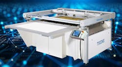
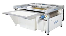
Initially, screen printing borrowed from the publishing markets allowed for flexible job-shop production of printed flexible sensors on individual substrate sheets. This process remains a staple today, supported by modern flatbed screen presses such as the Thieme 3000, which offers improvements in automated sheet feeding, cleaning, alignment, inspection, and conveying to dryers (Fig. 2).
Adoption of rotary screen methods can increase production throughput at the expense of print resolution. And thanks to direct-to-screen printing advances, rapid changeover from one type of sensor to another can reduce setup times by enabling on-the-fly creation of screen emulsion masks.
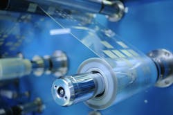
More recently, high-speed roll-to-roll machinery (Fig. 3) has migrated from publishing to printed electronics markets. However, it currently remains limited to sensors with minimal print-to-print variation, while end of roll batch testing (often in kilometer lengths) can create challenges in assuring overall yields when something goes wrong. Printing onto substrate rolls can be achieved by a variety of methods, including slot die coating, flexographic, gravure, ink jet, rotary screen, or other methods.
In-line electrical or visual image quality testing is challenging and expensive at high roll speeds, and if speeds are reduced to enable such in-line testing, then it reduces the volume efficiency advantage over traditional screen printing. Moreover, print resolution varies with speed as well, such that finer resolution requires slower production rates.
Additive printing techniques are being increasingly applied to printed flexible electronics to achieve more complex designs in low volumes, including 3D, aerosol jet, or impulse printing. With additive printing, complex layers of various substrates, conductive inks, and various sensing materials becomes possible.
While flexible electronics printing is the core process for thin-film sensor manufacturing, secondary operations continue to remain problematic for achieving high-throughput scale, including lamination, die cutting, pinning or connectorization, packaging, and testing. Continued investments in automation, e.g., automated pinning, digital rotor die cutting, robotic assembly and test, CCD image analysis, in-line flying probe testing, and other innovations, will help achieve higher efficiencies and scale.
Companies such as Tekscan are partnering with an ever-growing range of equipment suppliers and printed electronics contract manufacturers to mix and match new designs with appropriate production methods and volumes for various sensor designs.
The advancement of manufacturing techniques enables production of a broader variety of sensor designs, serving a larger market footprint over time. It also facilitates high-volume and low-cost consistent production of specific types of sensors, favorable for large-scale embedded applications.
Innovation in High-Volume Manufacturing
Strain gauge, resistive, piezoresistive, and capacitive thin-film sensor currently dominate the high-volume market landscape due to design and production simplicity and cost (Fig. 4).
Sensor performance trends observed include:
- The need for both smaller and larger sensor surface areas.
- Higher and lower sensing resolutions (the latter seeking to reduce costs at the expense of resolution)
- Simplified signal processing or electronics to reduce costs and power.
- Wider operating environments (temperature, humidity, harsh environments, etc.).
Innovative manufacturing methods will enable new, and more complex, technologies to find their initial foothold in market applications with potential further growth. For example, multimodal sensors, which can measure pressure and temperature simultaneously, are in demand for industrial and energy applications, while “micro-sensors” are increasingly designed into consumer or medical electronics applications.
There’s a growing market for flexible and stretchable sensing materials that can be integrated into smart textiles and conform to irregular or dynamic surfaces such as vehicle seating. Design and manufacturing of flexible and stretchable sensors are challenging due to dynamic changes in conductive or resistive inks, which may cause hysteresis, drift, or other performance issues over time. Moreover, wearable sensors require low power consumption, favoring certain technologies like piezoresistive sensing.
Embedding Sensors in Product Design
The growing ubiquity of tactile sensing for embedded applications is driving further improvements in integration, connectivity, and application intelligence. Large-scale sensor deployment requires standardization and ease of integration using simplified electrical signal processing to reduce costs, as well as the availability of modular firmware and software toolsets for varied applications.
In the case of mapping sensors (such as pressure or temperature mapping profiles), open-source tools are now readily available for image interpretation borrowed from visual and infrared camera image analysis routines.
Pressure and Force Sensor Integration: Considerations and Best Practices
When it comes to successful integration of tactile sensors into commercial devices, one of the most critical factors is how well the sensor is embedded into the larger system — electrically and mechanically. Engineers must evaluate not only signal accuracy and range, but also power constraints, circuit complexity, environmental durability, and the ease of calibration and production scaling.
One example of this system-level thinking is the approach Tekscan recommends to engineers integrating its FlexiForce tactile force sensors. These resistive sensors are widely adopted for embedded force measurement in medical, industrial, and consumer applications.
Achieving consistent and reliable results with any tactile sensor depends heavily on proper electrical and mechanical integration. Each technology has its own nuances, and the sensor manufacturer should be able to advise on a structured approach to help save time and costs in integration.
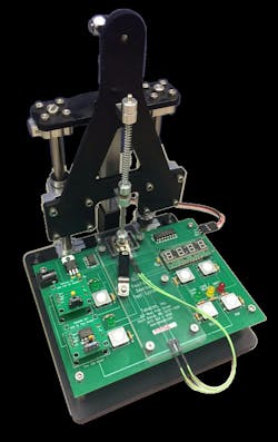
The initial phase involves sensor characterization, when engineers establish how the sensor performs under controlled force inputs. One way to do this is by using a desktop loading fixture with a known load cell reference (Fig. 5). This step allows the team to evaluate signal stability, hysteresis, linearity, and repeatability. Circuit selection begins here as well, often starting with a simple voltage divider. While not linear at high loads, this circuit provides a quick, low-cost starting point.
At times, designers who are trying to leverage sensor performance will utilize more advanced circuits to achieve linearity over a greater dynamic range. Though they improve performance, op-amp circuits can introduce a tradeoff: additional cost and complexity to system electronics (Fig. 6).
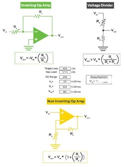
For instance, inverting op-amp configurations provide excellent linearity through zero and perform well across wide force ranges, while non-inverting op-amps offer strong linearity through an offset, suitable for more moderate ranges. All three circuits support sensitivity tuning through resistor or potentiometer adjustments, and engineers are encouraged to keep reference voltages between 0.25 and 0.75 V to optimize resolution and minimize power.
Once basic functionality is confirmed, the process moves into proof-of-concept prototyping. Here, the sensor is embedded into the intended mechanical environment—be it a housing, seat, or device interface. Engineers evaluate whether the circuit performs consistently when real-world interface materials and form factors are introduced. This stage is critical, as mechanical design (load concentration, puck materials, and even adhesive selection) can significantly influence electrical output.
From there, design teams typically develop a more advanced prototype, complete with calibration routines. Tekscan, for example, offers a Prototyping Kit to help streamline this phase, allowing teams to apply known force levels and build a two- or three-point calibration curve.
A common best practice is to load the sensor to 120% of its maximum expected force several times before calibration. This “conditioning” process helps stabilize sensor behavior. Sensitivity is typically set so that 100% of applied force produces about 90% of full-scale output, leaving room in the signal range to accommodate unexpected increases in force.
Following calibration, the next phase involves application and field testing to validate performance in real-world conditions. In one deployment involving infusion pump prototypes, the engineering team discovered that inconsistencies in sensor output were caused not by the sensor or circuit, but by a humidity-sensitive adhesive that interfered with load transmission. This example underscores the critical connection between mechanical and electrical design — and the need for thorough, system-level validation during integration.
After application and field testing is complete, it’s time to finalize the embedded design for production. At this point, teams are locking in resistor values, documenting calibration procedures, and ensuring consistent electrical output across units. This step ensures long-term repeatability and smooth transition into production scaling
Such a structured integration process reflects best practices in integrating tactile sensors and emphasizes a critical point: While sensor selection is important, the integration and validation workflow is just as critical. Reliable performance depends not only on sensor specifications, but on careful attention to system-level design, electrical and mechanical integration, thorough testing, and proper calibration.
>>Check out the other parts of this series
About the Author

John Jutila
CEO, Tekscan
John Jutila is CEO of Tekscan, a global leader of tactile sensor solutions. John previously held CEO positions at Ripley Tools, a supplier of infrastructure installation solutions, and Champion ONE, an optical networking technology company, as well as several positions at Nokia, including VP Strategy & Operations for Global Strategic Alliances, COO of the Strategic Industries Division EMEA Region, and North American Division President for Optical Fiber solutions.
John has also held key executive positions at Asahi Kasei/Polypore for microporous membrane technology, InterDigital for advanced mobile phone technology, and HP/EDS for IT outsourcing. He holds a DBA from Grenoble Ecole de Management, an MBA from the University of Toledo, and a BBA in Venture Management from The Wharton School.
Comment About the Article
To join the conversation, and become an exclusive member of Electronic Design, create an account today!

Leaders relevant to this article: