Aging-Aware Dynamic Frequency Management for Modern FinFET FPGAs
What you'll learn:
- How modern FinFETs actually age.
- The cost of static guardbanding.
- Reclaiming margin and giving it back over time.
- Industrial deployment.

Every FPGA shipped today is conservatively rated. The clock frequency on the datasheet is set so a worst-case die, at the worst voltage corner and temperature near the end of rated life, still meets timing. For most dies in their early lives, that rating is far below what the silicon could actually deliver.
Vendors do this because static guardbanding is the only way to make a reliability promise that survives the field9,10 and the cost is real: performance and energy efficiency persistently left on the table. With bias-temperature instability (BTI) and hot-carrier injection (HCI) now well characterized in FinFET technologies,1,2,4 that cost is becoming hard to justify. This article describes a closed-loop, learned frequency controller that reclaims most of the static margin in a device's early years, hands it back as it ages, and stays inside the reliability envelope at every step.
How Modern FinFETs Actually Age
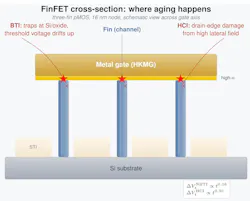
Two mechanisms dominate intrinsic FinFET aging at the operating voltages used by current 14- and 16-nm fabric. Negative bias temperature instability creates traps at the silicon-dielectric interface under sustained gate stress, shifting the pMOS threshold voltage upward over time.4,5 Hot-carrier injection generates damage near the drain edge under high lateral fields, predominantly in nMOS devices.
Both have been characterized extensively in production replacement-metal-gate FinFET stacks1,2 and measured directly on 16-nm FinFET FPGA fabric.3 Figure 1 shows where each mechanism does its work in a three-fin pMOS cross-section.
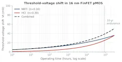
BTI kinetics in modern FinFETs follow a power law in stress time with a fractional exponent of 0.14 to 0.18.1,2 HCI follows a steeper power law, typically 0.25 to 0.35. Combined, they produce the threshold-voltage drift in Figure 2, calibrated against published 16-nm FinFET technology data.3 The headline observation is that the device isn’t stress-free in its early life and not catastrophically degraded at end of life. There’s a long, mostly linear region in log-time where a controller has both opportunity and accountability.
From Vt Shift to Slack Erosion
The threshold-voltage shift translates almost directly into timing slack. A 40-mV pMOS Vt shift produces tens to hundreds of picoseconds of setup-time degradation on a typical critical path in 16-nm fabric, depending on logic depth, fanout, and voltage. Direct ring-oscillator measurements on 16-nm FinFET FPGAs corroborate this scale.3
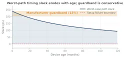
Figure 3 shows the worst-case path slack of a representative FPGA design over a 10-year window. The shaded band at the top is the manufacturer's static guardband, conventionally about 15% of nominal frequency. In the early years, the guardband was much larger than the actual erosion — such a gap is the headroom that can be reclaimed by a controller. Most of the performance gap between datasheet and silicon lives in the first three years of a device's life. That’s where a learned controller pays for itself.
The Cost of Static Guardbanding
Figure 4 plots achievable maximum frequency as a function of junction temperature for a fresh device and the same device after five years of stress. The grey dashed line is the static guardbanded fmax, set so that the worst-aged corner still meets timing at the worst temperature. The shaded band between the two curves is capability that’s never exposed by the static rating; for a fresh device, everything above the grey line is performance left on the table.
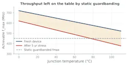
For example, a design that runs at 720 MHz when fresh and 500 MHz after five years, but it’s rated at 450 MHz throughout, costs the operator both throughput and joules. Dynamic voltage and frequency scaling (DVFS) on commercial FPGAs has been explored for two decades,6,7 including low-power FPGA devices,8 but those schemes lack a principled aging budget: They recover headroom against process and temperature without modeling the BTI and HCI cost of operating above the static rating.
ARES: A Learned Aging-Aware Controller
ARES (Adaptive Reinforcement-learned Energy Scheduler) is an on-chip clock manager that observes a small telemetry vector, chooses an operating point from a discrete frequency-voltage table, and is rewarded for throughput while penalized for energy, SLA misses, and aging. Adaptive frequency and biasing techniques driven by on-die sensors have a long history in production silicon.11,12 ARES replaces the hand-tuned controller with a learned policy15 that internalizes the aging cost.
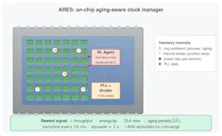
Figure 5 sketches the architecture: on-die ring oscillators (process and aging sensors), thermal diodes, and per-rail power measurements feed a soft-actor-critic (SAC) policy14 on an embedded MCU adjacent to the fabric, whose action sets the phase-locked-loop (PLL) target frequency. Sampling runs every 10 ms with one-second episodes.
State, Action, and the Aging-Aware Reward
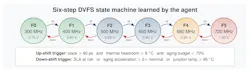
The state vector is small and physical: ring-oscillator frequency (a proxy for instantaneous process and aging), junction temperature, supply voltage, queue depth, and an aging-credit counter integrating voltage-temperature stress. The action space is the six-step DVFS table in Figure 6. The reward is a positive throughput term minus three penalties: energy per step, an SLA-miss count (one-bit setup-time violation flags from in-fabric detectors of the kind in Reference 12, summed across the fabric), and an aging-penalty proportional to estimated incremental ΔVt.
SLA misses are driven to zero in normal operation: Any nonzero count triggers an immediate frequency step-down rather than being tolerated as functional bit errors. The aging-penalty constant is calibrated per-lot during characterization so that cumulative ΔVt over rated life stays inside a 40-mV budget with a 10% safety margin. Without this penalty, a naive reinforcement learning (RL) agent would run at maximum frequency and voltage continuously, optimizing today's throughput at the cost of next year's silicon.
Training and Convergence
Training was performed in a simulator calibrated against published 16-nm FinFET BTI and HCI models,1,2 with ring-oscillator measurements from comparable 16-nm fabric used to calibrate the aging coefficients.3 A development-board harness on a Stratix-class part verifies that the full telemetry-to-action loop runs in under 2 ms on the embedded MCU, well inside the 10-ms sampling window; long-duration silicon aging measurement is future work.
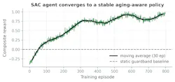
Figure 7 shows the composite reward over 800 training episodes. The agent crosses the static-guardband baseline within 60 episodes and stabilizes around episode 350.
Reclaiming Margin and Giving It Back Over Time
The behavior learned by the agent is the most useful result. Figure 8 plots operating frequency over a 10-year window. Early in life, the policy runs well above the static guardband, recovering the headroom the conservative rating gave away. As the aging counter grows and the ring oscillator slows, the agent gradually steps the operating frequency down toward the guardband — aggressive when the silicon is fresh, conservative when it has earned the conservatism.
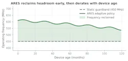
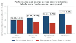
Figure 9 compares ARES against three baselines on a representative mixed-DSP workload (FIR filters, FFTs, and INT8 GEMMs at varying load): a static guardband, a worst-case DVFS scheme that uses the datasheet voltage-frequency table without telemetry, and an aging-aware adaptive frequency scheme in the style of that in Reference 11. ARES achieves 1.46X the throughput of the static guardband at 0.66X the energy per operation. The savings come from running fewer overprovisioned cycles at high voltage when the workload doesn’t need them.
Silicon population variance is critical for any vendor-facing claim. Figure 10 shows the distribution of reclaimed frequency margin across 96 simulated dies drawn from three fabrication lots. Mean reclamation is 28% with a standard deviation of 5.1%; no die falls below 15%, and none exceeds 39%.
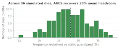
Lot-to-lot means stay within 1.5% of the population mean, and per-lot spreads overlap heavily; thus, within-lot process variation dominates over systematic lot bias. The narrow distribution matters more than the headline number. It tells the operations team that the controller behaves predictably across the silicon population.
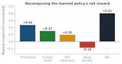
Figure 11 decomposes the steady-state reward into its components. The largest positive contribution is throughput, followed by energy savings and SLA adherence. The aging penalty is meaningful but small, which is the design intent: The agent accepts a measurable aging acceleration in exchange for a larger throughput and energy benefit, but it never trades reliability for performance in a way that would shorten the rated lifetime.
Industrial Deployment
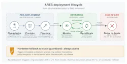
A learned clock controller is a hardware-adjacent closed-loop system with real safety stakes. Deployment follows the staged path in Figure 12, mirroring cautious rollout practice for learned controllers in other domains.13 Each silicon lot is characterized for BTI and HCI coefficients and ring-oscillator-to-Vt mappings; the agent is pre-trained on the calibrated simulator and fine-tuned on the device under monitored conditions; field monitoring continues throughout life.
On-chip cost is modest: The agent compute fits on a hardened MCU adjacent to the fabric, the telemetry path uses under 1% of host fabric resources, and combined idle power overhead is under 150 mW, roughly 2% of typical operating power for a mid-range FPGA.
The lifetime budget for the aging-credit counter is set to 40 mV ΔVt (the 10-year endurance point in Figure 2) with a 10% safety margin calibrated per-lot, which keeps the device inside its rated specifications over its full service life. Recalibration runs quarterly during the first year and annually thereafter, or immediately following any sustained junction-temperature excursion above 95°C.
If the learned policy exhibits unexpected behavior, such as sustained frequency oscillation, repeated SLA miss bursts, or divergence between the ring-oscillator trajectory and the calibrated aging model, the hardware fallback is asserted, and the device reverts to static guardband. The fallback is a hardware watchdog with a 100-ms timeout, reset by a periodic heartbeat from the agent, rather than a software check. Therefore, it remains effective even if the agent has failed. Field-reported anomalies trigger a model refit that propagates through the next recalibration cycle.
Outlook
Two developments will sharpen this work. The first is the spread of native on-die aging sensors, which removes the dependence on ring-oscillator inference. The second is the convergence of clock-management RL with thermal-management RL: temperature, frequency, voltage, and aging are coupled, and separate control surfaces leave joint optimizations unaddressed. The reclamation figures here are for compute-bound DSP and inference workloads. Memory-bandwidth-bound designs, where interface timing is the bottleneck, will see smaller gains.
For safety-critical applications such as aerospace and medical electronics, certifying a learned controller in the timing loop remains an open question. Conservative deployments will likely keep static guardband. For everyone else, the clock-control plane is becoming an active reliability surface. The datasheet number was an open-loop promise. The closed-loop number is what the device can actually deliver, all the way to retirement.
References
1. N. Parihar, U. Sharma, R. G. Southwick, M. Wang, J. H. Stathis, and S. Mahapatra, "Ultrafast measurements and physical modeling of NBTI stress and recovery in RMG FinFETs under diverse DC-AC experimental conditions," IEEE Trans. Electron Devices, vol. 65, no. 1, pp. 23–30, Jan. 2018. doi: 10.1109/TED.2017.2773122.
2. N. Parihar, N. Goel, S. Mukhopadhyay, and S. Mahapatra, "BTI analysis tool: Modeling of NBTI DC, AC stress and recovery time kinetics, nitrogen impact, and EOL estimation," IEEE Trans. Electron Devices, vol. 65, no. 2, pp. 392–403, Feb. 2018. doi: 10.1109/TED.2017.2780083.
3. J. Sobas and F. Marc, "Degradation measurement and modelling under ageing in a 16 nm FinFET FPGA," Micromachines, vol. 15, no. 1, art. 19, Dec. 2023. doi: 10.3390/mi15010019.
4. J. H. Stathis, S. Mahapatra, and T. Grasser, "Controversial issues in negative bias temperature instability," Microelectronics Reliability, vol. 81, pp. 244–251, Feb. 2018. doi: 10.1016/j.microrel.2017.12.035.
5. D. K. Schroder, "Negative bias temperature instability: What do we understand?," Microelectronics Reliability, vol. 47, no. 6, pp. 841–852, June 2007. doi: 10.1016/j.microrel.2006.10.006.
6. C. T. Chow, L. S. M. Tsui, P. H. W. Leong, W. Luk, and S. J. E. Wilton, "Dynamic voltage scaling for commercial FPGAs," in Proc. IEEE Int. Conf. Field-Programmable Technology (FPT), Singapore, Dec. 2005, pp. 173–180. doi: 10.1109/FPT.2005.1568542.
7. J. L. Nunez-Yanez, M. Hosseinabady, and A. Farhadi Beldachi, "Energy optimization in commercial FPGAs with voltage, frequency and logic scaling," IEEE Trans. Comput., vol. 65, no. 5, pp. 1484–1493, May 2016. doi: 10.1109/TC.2015.2435771.
8. T. Tuan, A. Rahman, S. Das, S. Trimberger, and S. Kao, "A 90-nm low-power FPGA for battery-powered applications," IEEE Trans. Comput.-Aided Design Integr. Circuits Syst., vol. 26, no. 2, pp. 296–300, Feb. 2007. doi: 10.1109/TCAD.2006.885731.
9. S. M. Trimberger, "Three ages of FPGAs: A retrospective on the first thirty years of FPGA technology," Proc. IEEE, vol. 103, no. 3, pp. 318–331, Mar. 2015. doi: 10.1109/JPROC.2015.2392104.
10. S. Borkar, "Designing reliable systems from unreliable components: The challenges of transistor variability and degradation," IEEE Micro, vol. 25, no. 6, pp. 10–16, Nov.-Dec. 2005. doi: 10.1109/MM.2005.110.
11. J. Tschanz, N. S. Kim, S. Dighe, J. Howard, G. Ruhl, S. Vangal, S. Narendra, Y. Hoskote, H. Wilson, C. Lam, M. Shuman, C. Tokunaga, D. Somasekhar, S. Tang, D. Finan, T. Karnik, N. Borkar, N. Kurd, and V. De, "Adaptive frequency and biasing techniques for tolerance to dynamic temperature-voltage variations and aging," IEEE ISSCC Dig. Tech. Papers, San Francisco, CA, USA, Feb. 2007, pp. 292–293. doi: 10.1109/ISSCC.2007.373409.
12. K. A. Bowman, J. W. Tschanz, N. S. Kim, J. C. Lee, C. B. Wilkerson, S.-L. L. Lu, T. Karnik, and V. K. De, "Energy-efficient and metastability-immune resilient circuits for dynamic variation tolerance," IEEE J. Solid-State Circuits, vol. 44, no. 1, pp. 49–63, Jan. 2009. doi: 10.1109/JSSC.2008.2007148.
13. V. Mnih, K. Kavukcuoglu, D. Silver, A. A. Rusu, J. Veness, M. G. Bellemare, A. Graves, M. Riedmiller, A. K. Fidjeland, G. Ostrovski, S. Petersen, C. Beattie, A. Sadik, I. Antonoglou, H. King, D. Kumaran, D. Wierstra, S. Legg, and D. Hassabis, "Human-level control through deep reinforcement learning," Nature, vol. 518, no. 7540, pp. 529–533, Feb. 2015. doi: 10.1038/nature14236.
14. T. Haarnoja, A. Zhou, P. Abbeel, and S. Levine, "Soft actor-critic: Off-policy maximum entropy deep reinforcement learning with a stochastic actor," Proc. 35th Int. Conf. Machine Learning (ICML), PMLR, vol. 80, Stockholm, Sweden, July 2018, pp. 1856–1865.
15. R. S. Sutton and A. G. Barto, Reinforcement Learning: An Introduction, 2nd ed., Cambridge, MA, USA: MIT Press, 2018.
>>Download the PDF of this article
 dreamstime_justlight_465377220
About the Author
Saher Elsayed
Graduate Teaching Assistant, School of Engineering and Applied Science, University of Pennsylvania
Saher Elsayed is a Graduate Teaching Assistant at the School of Engineering and Applied Science, University of Pennsylvania.
Comment About the Article
To join the conversation, and become an exclusive member of Electronic Design, create an account today!
 Leaders Logo
Leaders relevant to this article: