Overcome Miniaturization Obstacles Through Cross-Disciplinary Design

This article is part of the TechXchange: Critical Connections: Cables, Wires, Vias, and Busbars.
What you'll learn:
- Why cross-disciplinary innovation works best in miniaturization efforts.
- How changes in board connections are creating new design challenges.
- Rethinking connector layouts to overcome those challenges.
Ever since Gordon Moore predicted in 1965 that the number of transistors on computer chips would double every two years, the electronics industry has diligently pursued this roadmap with astonishing accuracy. Now, more than a half century later, what’s become known as Moore’s Law has established a steady pace of computational progress, resulting in generations of increasingly smarter, faster, and smaller electronics.
When IBM unveiled its 2-nm chip technology in 2021, it was heralded as a major breakthrough for the entire semiconductor industry. The ability to place 50 billion transistors onto a space about the size of a fingernail is projected to achieve 45% higher performance or 75% lower energy use than the most advanced 7-nm node chips.
For product designers, this transformative technology is intended to quadruple cell-phone battery life, slash data-center carbon footprints, accelerate laptop functions, and speed reaction time in autonomous vehicles. Simply put, smaller, faster, higher-efficiency chips give designers many more options to increase product performance.
However, designers must first clear a growing set of obstacles that require new levels of cross-disciplinary problem-solving to meet relentless demands for more powerful components and products in ever-shrinking form factors.
Cross-Discipline Product Design: Benefits and Tradeoffs
The most critical factor facing product designers today is finding the right balance between functional benefits and operational tradeoffs. This necessitates a stringent evaluation of different design considerations to determine the potential impact of each new feature or function on mechanical performance, operability, and reliability.
Equally important is identifying any potential problems with electrical performance, like achieving higher speeds and frequencies with lower power consumption and latency.
Savvy designers are embracing a more specialized approach that involves creating a team with cross-discipline skills and expertise well-versed in navigating and negotiating unforeseen challenges dealing with smaller spaces and shapes. Tackling a laundry list of miniaturization challenges requires an “all hands on deck” approach with mechanical, electrical, and thermal engineers participating in the process from the beginning.
Hands-on experience with the latest manufacturing process innovations and automation is crucial. That’s because many components now are too small to be placed by hand, which requires specialized knowledge of highly automated manufacturing techniques.
It’s imperative for each stakeholder’s piece of the design puzzle to integrate seamlessly into one module/device. Each market has different tradeoffs with respect to miniaturization. In the world of data centers, data speeds are the predominant concern whereas robustness reigns supreme in industrial and consumer device products.
In the mobile-phone market, for instance, the promise of 5G is intensifying demands for miniaturization, primarily because 5G-related capabilities require more power and, therefore, bigger batteries. As pressure builds to shrink other components, engineers are responding with ever-smaller RF connectors, as well as connectors of different heights to offer greater flexibility in component placement.
Connector Development Case Study
When Molex set out to develop its Flex-to-Board RF mmWave Connector 5G25 Series, a global team of specialists leveraged experience in RF and antenna design, high-speed connectivity, and volume manufacturing to support 5G’s higher frequencies while raising the bar in signal stability, robust performance, and fast assembly. The result of this end-to-end, holistic product design approach was the development of a space-saving solution designed to meet the demands of 5G millimeter-wave (mmWave) applications up to 25 GHz.
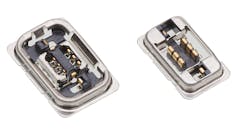
Among the many obstacles they faced was the strict requirement to avoid signal leakage, which led to the development of new gap-free manufacturing methods, as well as full electromagnetic-interference (EMI) shielding for optimal signal integrity. To accomplish this, the team combined traditional design and manufacturing rules with more innovative and collaborative design methodologies. This approach helped alleviate common issues that are prevalent at higher speeds, such as signal loss, interference, and crosstalk.
Achieving a strategic balance of critical electrical, mechanical, and environmental requirements enabled the team to provide working prototypes within months. That was followed by rapid ramping up of volume manufacturing to produce five million connectors per month on behalf of a leading smartphone manufacturer.
At each design step, an exchange of ideas and performance simulations made it possible to advance both electrical and mechanical performance. Meanwhile, manufacturing engineers ensured that molding, stamping, and plating were ramped and ready for volume manufacturing.
Risk management was addressed collectively as designers shared different experiences to find common threads and learn from each other. Understandably, each process or function has its own design rules, including some margins that must be considered. Accelerating miniaturization, however, requires reducing risk across the entire system or process, which is enhanced by taking advantage of insights and ideas gleaned from other industries.
The rise of electric vehicles is another trend creating demand for lighter electronics. Massive industrial equipment can benefit from tiny sensors residing on weight-sensitive robotic arms, while rising bandwidth needs in corporate data centers is driving major advances in fine-pitch interconnects.
Designers and engineers focusing on connected healthcare applications also need highly specialized knowledge on miniaturization. Meanwhile, those focused on mobile and/or wearable devices might have the most insights into creating high-density and complicated functionality.
The Miniaturized Connector Conundrum
Among the seemingly endless list of design challenges and tradeoffs spurred by momentum in miniaturization is how connections between boards and components are changing. Electrical connectors play a vital role in product design while offering myriad options in terms of wire-to-board, wire-to-wire, board-to-board, flexible flat cable (FFC), flexible printed circuit (FPC), input/output (I/O), power, and radio-frequency (RF) connectivity. As overall designs shrink, so must connectors.
Miniaturized connectors play an understated but make-or-break role in many of today’s solutions, delivering rising levels of mate-ability, robustness, contact reliability, current capacity and solderability. The task isn’t without its obvious challenges.
Though smaller connector pins make higher-frequency signals potentially available, it can be hard to balance this with mechanical performance. In addition, smaller connector footprints can create signal interference between high-speed and RF signals. Multiple tradeoffs must be weighed, as size directly correlates with performance. Mechanical limits also come into play as connectors in the automotive sector, for example, must be robust, waterproof, and vibration-proof.
To that end, designers are getting increasingly creative about connector layouts instead of continually trying to shrink connector size. Last year, Molex announced its Quad-Row Board-to-Board Connectors, which have a staggered-circuit layout that produces a 30% space savings over conventional connector designs.

A long-standing collaboration with product developers from a major smartwatch manufacturer led to this design, which positions pins across four rows at a signal contact pitch of 0.175 mm. In addition to the space savings, the design enables high-density circuit connectivity, suiting it for space-constrained smartphones, smartwatches, medical wearables, and augmented-reality/virtual-reality (AR/VR) devices.
Wearable devices are among the leaders when it comes to meeting the toughest requirements for miniaturization. This segment demands that new functionality is embedded in exceedingly small packages, so design efforts for a lower profile and shorter length are always required.
For next-gen RF connectors, the toughest obstacles are delivering higher speed/frequency, signal integrity like impedance matching, and isolation performance while balancing mechanical performance—all in a smaller footprint. Emerging applications will continue to spur advances in next-gen connector designs.
The principles of design for manufacturability are already being challenged by applications that demand connectors the size of a grain of rice. Manufacturers that take the lead here are applying fully automated processes that include multiple vision-inspection systems to ensure accurate dimension management.
As the eventual demise of by-hand assembly methods gets closer, manufacturers must respond by adopting robot-centric assembly methods and gradually expanding them. The momentum of miniaturization isn’t the only motivator, as manufacturers must abide by stringent quality assurance program (QAP) improvements. At the same time, as module costs become more expensive due to the need for higher functionality, failure rates in the assembly process increase per-device costs. As a result, more robust connectors sometimes are required, not just to pursue miniaturization.
To alleviate the conundrum of designing critical connection points, engineers should involve mechanical and connector experts much earlier in the system/architecture design phase. This not only will reduce connectivity complexities, but it can result in noticeable contributions to optimize the entire system design, including cost and manufacturability.
A Team Miniaturization Effort: Put Innovation into Action
The best route for minimizing tradeoffs surrounding cost, space, connectivity, and functionality involves engineers coming together to prioritize what they need to achieve within acceptable windows. Relying on novel processors, with higher pin counts and increasingly smaller connectors, may be a sustainable answer for meeting short-term demands, but it won’t be the right approach for the long haul.
In some cases, it won’t be possible to extend the trajectory of existing technologies. Therefore, new ones must be created to deliver products that are capable of ultra-low power consumption, high-speed signal processing, and the fusion of VR aided by sophisticated predictions technologies.
NTT Group is striving to do that with the development of its Innovative Optical and Wireless Network (IOWN) concept. It aligns the work of nearly 30 other companies, including Intel and Sony, to develop an all-photonics network that incorporates optical technologies at every level—from networking to devices, and even inside chips.
Right now, though, if a miniaturized connector is available for higher speeds, and if some digital signals can be integrated into one higher signal, the demand might be feasible by applying a serializer/deserializer (SerDes) chip. This is just an option, of course, but developing other potential alternatives would be required to sustain innovation.
Clearly, dealing with the nuances of miniaturization is a team sport, so product designers who relish collaboration will become increasingly vital for driving new product and connectivity innovations while addressing power management, signal integrity, and manufacturability. When a cadre of engineers understands deeply the reasons why innovation is required, they can focus on developing a multitude of alternatives, denoting the pros and cons for each.
Physics Finish Line: What Comes Next?
As the industry gets closer and closer to reaching the limits of physics, it becomes increasingly expensive—if not impossible—to shrink further. So, what will Moore’s Law be replaced with? In the short term, specialty chips are more frequently designed for each function, such as AI accelerators, GPUs, or video accelerators. These chiplets are then used in 2D- or 3D-stacked multichip modules. Looking further out, some of the solutions under consideration are design quantum computers, using memristors or graphene processing.
While timing and tradeoffs for miniaturization will continue to vary depending on products, industry sectors, and partner ecosystems, there are universal truths that apply across the board. In all cases, it comes down to determining the best path forward with a keen eye on creating value while containing costs by applying the right mix of engineering, planning, and manufacturing expertise and experience.
Read more articles in the TechXchange: Critical Connections: Cables, Wires, Vias, and Busbars.
About the Author
Mike Deppe
Vice President of Global Product Development, Molex
Mike Deppe is Vice President of Global Product Development at Molex. Previously, he was Vice President & General Manager for Molex RF & Printed Circuit Solutions Business Units. He has over 20 years of experience in printed electronics and automated assembly and leads Molex’s global efforts to be the preferred partner for components, interconnect, and assemblies that enable innovation and commercialization of RF technologies.
Mike has held various progressive roles in Engineering, Project Management, and Operations overseeing facilities in Taiwan, China, Canada, and the U.S. He led product development responsibilities for human-machine interface (HMI) assemblies, copperflex products, printed electronics, and sensor systems, where he managed and steered the development efforts in advancing manufacturing, processing, and capabilities of hybrid electronics.
Mike earned degrees in Mechanical Engineering and Economics from Purdue University.
Comment About the Article
To join the conversation, and become an exclusive member of Electronic Design, create an account today!

Leaders relevant to this article: