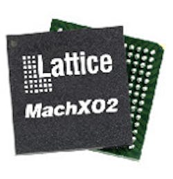
65nm MachXO2 PLDs
MachXO2 PLD family
Control dev board
PLDs often play second banana to FPGAs. Lattice Semiconductor's low cost, low density MachXO2 (Fig. 1) PLDs aim to change that view. They are based on Lattice Semiconductor's 65nm flash process technology that provides a 3x increase in logic density, a 10x increase in embedded memory, and a 100X reduction in static power. All this along with a 30% cost reduction versus the original MachXO PLD family. A triple staggered I/O architecture increases the number of i/O pins. BGA packaging reduces footprint size. The chips come in package sizes (Fig. 2) ranging from 2.5mm by 2.5mm to 14mm by 14mm. Power requirements range from 19uW to 230uW depending upon the number of LUTs (lookup tables).
The MachXO2 incorporates hard timer, I2C and SPI interfaces. This can save up to 600 LUTs. The chips also have an on-chip oscillator. Chips are available in low power, 60MHz versions and high performance 150MHz versions. The latter can include an on-chip voltage regulator.
Lattice Semiconductor provides a wide range of IP for the MachXO2. These range from LPC bus controllers to flash and DRAM controllers. There are even display controller interfaces available. An asymmetrical banking scheme maximizes I/O usage while providing multiple interface power supply voltage regions.
Development is handled by Lattice Semiconductor's new Lattice Diamond development tool. It is integrated with Aldec and Synopsis Synplicity synthesis and simulation support.
Pricing starts at $0.75. The high end LCMXO2-1200ZE/HC is priced at $2 and comes in a TQFP100 package.
Lattice Semiconductor development kits for the MachXO2 will include a $99 Pico development board and a $149 Control development board (Fig. 3). The latter incorporates a power supply sequencing, temperature monitoring, fan control and fault logging. It also has a 7:1 LVDS display interace.
About the Author
William G. Wong
Senior Content Director - Electronic Design and Microwaves & RF
I am Editor of Electronic Design focusing on embedded, software, and systems. As Senior Content Director, I also manage Microwaves & RF and I work with a great team of editors to provide engineers, programmers, developers and technical managers with interesting and useful articles and videos on a regular basis. Check out our free newsletters to see the latest content.
You can send press releases for new products for possible coverage on the website. I am also interested in receiving contributed articles for publishing on our website. Use our template and send to me along with a signed release form.
Check out my blog, AltEmbedded on Electronic Design, as well as his latest articles on this site that are listed below.
You can visit my social media via these links:
- AltEmbedded on Electronic Design
- Bill Wong on Facebook
- @AltEmbedded on Twitter
- Bill Wong on LinkedIn
I earned a Bachelor of Electrical Engineering at the Georgia Institute of Technology and a Masters in Computer Science from Rutgers University. I still do a bit of programming using everything from C and C++ to Rust and Ada/SPARK. I do a bit of PHP programming for Drupal websites. I have posted a few Drupal modules.
I still get a hand on software and electronic hardware. Some of this can be found on our Kit Close-Up video series. You can also see me on many of our TechXchange Talk videos. I am interested in a range of projects from robotics to artificial intelligence.

