MicroLED Displays: How to Achieve a 99.9999% Yield
This article is part of the TechXchange: Advanced Display Technology.
What you’ll learn:
- The advantages of microLED over other display technologies.
- The manufacturing flow and where process control comes into play for microLED display fabrication.
- The challenges in manufacturing microLED displays.
- How advanced process control can help achieve 99.9999% yield.
Shifting to microLED display technology presents opportunities and challenges for manufacturers. In many ways, microLED is technologically superior to OLED (organic LED) and liquid-crystal display (LCD). It’s quite versatile and can be used in myriad form factors, outperforming other display technologies. Given its extremely small pixel size, microLED also frees up space on displays to include other components that can provide an improved user experience.
On the flip side, microLED display fabrication is costly and sophisticated, plus it requires exceptional quality control. High yield is imperative to make microLED displays economically feasible, but achieving this high yield is challenging.
Process control can provide manufacturers with a pathway to achieving six nines—99.9999% yield—at a reasonable cost. This is the only acceptable display yield for human eyes, highly sensitive to bad pixels and thus requiring near-perfect displays.
Advantages of MicroLED
MicroLED display technology has many advantages. It provides superior brightness, is more energy efficient, and lasts longer. Compared to OLED and LCD, microLED also offers better contrast and is more tolerant to moisture, vibration, and heat.
In terms of versatility, microLED can be used for form factors where other display technologies would not perform as well. Curved displays in automotive applications are a good example of a form factor where microLED will outperform others based on shape, brightness, and longevity.
And, as mentioned above, the extremely small size of a microLED—it covers only a fraction of a pixel area—allows for the addition of sensors, cameras, drivers, antennas, and the like, to enhance the capability of the display and/or the opportunity for transparent displays.
It’s the exceptionally high yield of six nines at a reasonable cost that stands in the way of microLED becoming a more widely used display technology. This high-yield requirement increases the cost of microLED displays, making them less attractive for consumer and other more mainstream applications.
Manufacturing Flow and Process Control for MicroLED
MicroLED display fabrication has a sophisticated process flow with process control required at each step (Fig. 1). In a simplified flow, it begins with the fabrication of the LEDs themselves, typically on sapphire or gallium-arsenide (GaAs) wafers with many epitaxial layers.
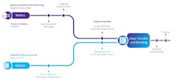
The unpatterned wafers require extensive process control for the substrate and epi layers to make sure they provide a high-quality starting point for the remainder of the processing. Subsequently, during the microLED formation, inline inspection and metrology helps drive both yield and uniformity improvements for the microLEDs. Once the microLEDs are fabricated, they must have outgoing quality control (OQC) to ensure that the product shipping to panel assembly sites meets all quality and yield requirements.
For some display designs, an optional driver integrated circuit (IC) is also fabricated on a silicon wafer. This uses a conventional complementary metal-oxide semiconductor (CMOS) process with a full range of inline inspection and metrology. Again, the optional driver IC requires an outgoing quality check to ensure that the driver IC meets the yield and parametric requirements.
Lastly, there’s backplane fabrication on glass panels using whichever thin-film transistor technology (TFT) is required for creating the pixel-driving circuitry. This fabrication step also has its own range of inline inspection, metrology, test, and repair needed to achieve the backplane quality stipulated.
Next, the components—microLEDs, driver ICs, and backplanes—are combined at the panel assembly site. Once incoming quality control is complete, mass transfer can take place. However, the mass-transfer process is extremely challenging. In the microLED display fabrication process, millions to hundreds of millions of parts are only tens of microns in size.
Manufacturers implement redundancy strategies that involve using multiples of microLEDs of the same color per pixel to ensure at least one of them is functional on the display to help improve final performance. Redundancy, though, multiplies the number of microLED source wafers required, which can be the largest single cost associated with this type of display.
As a result, it’s complex and expensive to manage the mass-transfer and bonding processes. Once the mass transfer and bonding are complete, the next step is a series of inspections and metrology, Light On electrical testing, and repair to achieve the final display quality desired.
Challenges of Manufacturing MicroLED Displays
Overcoming the significant cost and yield challenges in manufacturing microLED displays requires sophisticated process control as one of the key enablers. Therefore, inspection and metrology at critical steps of microLED display fabrication is paramount. We like to say, “You can't fix what you can't find, and you can't control what you can't measure.”
The final microLED display yield is a function of not only the microLED epi, patterning, and fabrication, but also of the backplane yield, as well as the transfer and bonding yield of the mass-transfer process required to assemble the components. All of these together result in the final display yield.
Figure 2 illustrates an example of the challenge: Assume 99.99% or four nines yield for the microLED fabrication process and transfer in bonding process, and then 99.9999% or six nines yield on the backplane for an 8K TV display with no redundancy. Even with these seemingly very high yields, the final display yield is 99.9799% and the number of repairs to achieve the required display yield is 20,000. Even if we add 2X redundancy into the process, about 100 repairs will likely be required, which would still add cost.
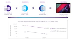
It’s necessary to achieve very, very high-yield values for each component in the display process to result in economical displays with reasonable repair levels. This is where advanced process control comes into play.
Using Advanced Process Control for 99.9999% Yield
Bottomline: Process control increases manufacturability and reduces cost. However, microLEDs require an entirely new level of process control like that used in the Si IC fabrication space. Manual control processes, like those used for conventional LEDs, will not produce the desired results.
Manufacturers should apply advanced process control with high-speed, high-sensitivity metrology and inspection. This will increase baseline yield for microLED displays and improve downstream processing, including repair.
Further improvements to yield and reductions in cost can be achieved with the application of advanced process tools that are designed for high-volume manufacturing. Inspection and metrology at every critical step in the process will let you fix what you find and control what you measure, ultimately improving the overall yield to levels that will allow this technology to be viable for consumer products.
For more background on microLED display technology, read “MicroLED Poised to Disrupt the Displays Market,” an interview with KLA Corp.’s senior principal scientist John C. Robinson.
Read more articles in the TechXchange: Advanced Display Technology.
About the Author
John C. Robinson
Senior Principal Scientist, KLA Corp.
John has 25+ years’ experience in the semiconductor industry in metrology, inspection, and process control, including applications engineering, product development, marketing management, and individual contributor roles. He has published over 60 technical papers and 20 patents, and is a fellow of SPIE.
Comment About the Article
To join the conversation, and become an exclusive member of Electronic Design, create an account today!

Leaders relevant to this article: