A Novel Approach to a New Type of Optics
What you'll learn:
- Insights from Myrias Optics on the technical and economic challenges facing traditional optics in AI data centers and other markets.
- Details on the company’s unique “wafer-level” optical manufacturing technology.
- What are metaoptics and how do they differ from traditional, refractive optics?
Optics are everywhere today, forming the front end of cameras used in consumer, industrial, and medical systems as well as waveguides used in augmented-reality (AR) glasses and extended-reality (XR) devices.
In data centers, too, pluggable optical transceivers translate electronic signals into photons and transfer them at high speeds before converting them back. They’re key for managing the massive amounts of data used by AI. Despite being small, the optics end up being indispensable to the total solution.
But across these markets, system designers are facing a similar bottleneck: Producing advanced optical components that combine high performance, durability, and scalable manufacturing economics.
Nanoimprinted All-Inorganic Metaoptics
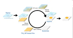
Electronic Design talked with John Fijol, CEO of Myrias Optics, about the company’s inorganic, nanoimprint lithography process that aims to address this challenge. Its wafer-level optics technology can implement a wide range of advanced optical systems, including diffractive optics and waveguides, that reduce size, weight, and part count compared to traditional refractive optics, especially in complex assemblies (see figure).
Besides its scale-up potential, the company said its inorganic, nanoimprint process enables high-precision optics with strong material performance. In AR glasses, for instance, high refractive index waveguides allow for wider fields of view while maintaining manufacturability. In data centers, similar material and process advantages help improve optical coupling efficiency, alignment tolerance, and thermal robustness in high-speed interconnects.
The startup can also manufacture metaoptics, a relatively new technology that puts planar optics directly on a chip. These advanced lenses use flat surfaces consisting of sub-wavelength structures — sometimes referred to as nanopillars — to manipulate light. According to Myrias, metaoptics deliver a degree of control that’s not possible with traditional refractive lenses, which use physically curved surfaces to bend and shape light.
Myrias said these components can also be tuned for all properties of light, including phase, wavelength, amplitude and polarization, and the metaoptics can combine several different optical functions in a single surface.
"Traditional polymer-based optical manufacturing presents limitations in durability, thermal stability, and long-term reliability," explained Jim Watkins, the startup’s founder and a professor of Polymer Science and Engineering at University of Massachusetts Amherst, in a press release. "By combining advanced metasurface design with robust inorganic materials and additive wafer-level processing, we are enabling optical components that meet the performance and supply chain demands of emerging AR, AI, and advanced imaging markets."
Only founded in 2021, Myrias is still in the early stages of commercialization. But the company said it’s focused on bringing its additive nanoimprint platform to market and expanding production capacity to meet growing customer demand.
In January, the startup raised $2.1 million in its latest seed round, bringing total funding to $6.9 million. The proceeds will support manufacturing scale-up, expansion of pilot production lines, and continued execution of customer programs. It also claims to be working with strategic partners and Tier-1 supply-chain companies to integrate its waveguide and metaoptics technologies into AR glasses, AI photonics, and advanced imaging systems.
About the Author

William G. Wong
Senior Content Director - Electronic Design and Microwaves & RF
I am Editor of Electronic Design focusing on embedded, software, and systems. As Senior Content Director, I also manage Microwaves & RF and I work with a great team of editors to provide engineers, programmers, developers and technical managers with interesting and useful articles and videos on a regular basis. Check out our free newsletters to see the latest content.
You can send press releases for new products for possible coverage on the website. I am also interested in receiving contributed articles for publishing on our website. Use our template and send to me along with a signed release form.
Check out my blog, AltEmbedded on Electronic Design, as well as his latest articles on this site that are listed below.
You can visit my social media via these links:
- AltEmbedded on Electronic Design
- Bill Wong on Facebook
- @AltEmbedded on Twitter
- Bill Wong on LinkedIn
I earned a Bachelor of Electrical Engineering at the Georgia Institute of Technology and a Masters in Computer Science from Rutgers University. I still do a bit of programming using everything from C and C++ to Rust and Ada/SPARK. I do a bit of PHP programming for Drupal websites. I have posted a few Drupal modules.
I still get a hand on software and electronic hardware. Some of this can be found on our Kit Close-Up video series. You can also see me on many of our TechXchange Talk videos. I am interested in a range of projects from robotics to artificial intelligence.

James Morra
Senior Editor
James Morra is the senior editor for Electronic Design, covering the semiconductor industry and new technology trends, with a focus on power electronics and power management. He also reports on the business behind electrical engineering, including the electronics supply chain. He joined Electronic Design in 2015 and is based in Chicago, Illinois.