DC-DC Converter Design Basics (Part 2): Boost Converters

This article is part of the Power Management series: DC-DC Converter Design Basics.
Members can download this article in PDF format.
What you’ll learn:
- The theory of boost converter operation.
- How to build boost converters using the SLG47105.
- Discover real-life examples where these devices can be used.
DC-DC converters are widely used to efficiently produce a regulated voltage from a source that may or may not be well-controlled to a load that may or may not be constant. Part 2 of this article series shows how the boost converter can be built using the Renesas SLG47105.
Boost Converter
Boost DC-DC converters, also called step-up DC-DC converters, are DC-DC power converters that increase the output voltage while decreasing the output current. They contain the same components as a buck DC-DC converter but are arranged in a different topology.
The relationships between input and output voltage, current, and power are as follows:
- UOUT > UIN
- IOUT < IIN
- POUT = PIN – PLOSS
Theory of Operation
When each cycle begins, FET 3 turns on and off for a fixed period (Fig. 1). The coil will generate a voltage spike with a higher amplitude than Vin. If the output voltage rises above the reference voltage, the cycle repeats but the FET 3 turn-on period is short enough to maintain the desired output voltage. FETs 3 and 4 turn on and off alternately, behaving like a typical synchronous boost regulator.
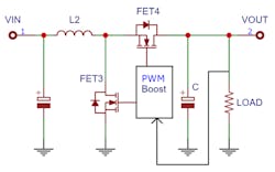
The duty cycle of FET 3 decreases until the minimum duty cycle of the converter in boost mode reaches 4%–6%.As an example, a simple boost converter was designed using the SLG47105 IC and Go Configure software (see below). It has the following parameters :
- Input voltage range (Vin): 2.7 to 4.5 V
- Output voltage: 5 V
- Output current range: 0.5 A − 1 A
- PWM frequency: 200 kHz
- Overcurrent/sort circuit protection: internal OCP
Calculated values:
- Min. duty cycle: 10%
- Max. duty cycle: 46%
- Min. inductor size: 1.7 µH (2.2 µH, 4 A rated)
- Peak inductor current: 3.7 A
- Filter capacitor (C): 100 µF (100-µF low ESR capacitor is recommended)
Go Configure Project
The regulator uses a 20-kHz clock like the previous one for the same reasons (Fig. 2). The boost pulse-width-modulator (PWM) logic is built on MF1 (CNT1/DLY1 and DFF 10) and 2-bit LUT1. The CNT1/DLY1 sets the minimum duty cycle of 1 %. It remains at a minimum until the feedback signal from the ACMP1H through the 2-bit LUT1 extends it to the width when the voltage on the feedback loop is equal to the Vref maintaining a constant load voltage.
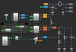
The HV OUT CTRL1 macrocell is configured as a fast-slew-rate half-bridge output. It has two half-bridge outputs that are connected in parallel to handle higher output current. Output pins (Pin 9 and Pin 10) are configured to «High and Low side on».
The ACMP1H in this design is used in a voltage feedback loop so that the PWM could stabilize the output voltage. The output voltage is determined by the ACMP’s Vref and the R1R2 voltage divider. In this case:
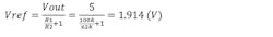
The closest Vref value available in the SLG47105 is 1920 mV, which is close enough.
Unlike in the buck design (see Part 1), it’s impossible using the HV OUT CTRL0 in the boost configuration. This is due to all internal logic circuits of both HV OUTs being powered from VDD 2A, and it can be used as voltage input only. On the other hand, VDD 2B powers only two high-side transistors of Pins 9 and 10. Thus, it can be used as a voltage output.
Conclusions
As can be seen, designing and building buck, boost, and buck-boost converters using the HVPAK SLG47105 chip is quite easy. The amount of unused macrocells leaves plenty of room for modifications and adding new features for proposed designs.
For example, a soft-start where a PWM period slowly increases from 0 to the required value reduces a peak startup current, programmable overcurrent protection, multiple output voltages, etc. Also, the HV OUT pins are suitable for driving external MOSFETs, which allows for building a very high-power DC-DC converter.
References
Circuit Design Software: Go Configure Software
Design Files: https://www.renesas.com/document/scd/cm-358-gp-file
About the Author
Nazar Sliunchenko
Technical Documentation Manager, Renesas Electronics
Nazar Sliunchenko graduated from National University "Lviv Polytechnic" in 2008, studying at the Department of Telecommunications, Radioelectronics & Electronic Engineering. He has more than 15 years of experience in hardware design, including analog and digital devices. Currently, Nazar is managing one of the Technical Documentation departments at Renesas Electronics Corp.
Comment About the Article
To join the conversation, and become an exclusive member of Electronic Design, create an account today!

Leaders relevant to this article: