This article is part of the TechXchange: Delving into EMI, EMC and Noise.
Members can download this article in PDF format.
What you'll learn:
- Ways to mitigate noise in SMPS.
- What to look for in PCB layout to reduce EMI.
- What are SSFD and DRSS?
Electromagnetic-interference (EMI) reduction techniques for power circuit designs are segmented into two categories: active and passive. Passive techniques focus on reducing the EMI level through various filtering techniques, adequate shielding, solid grounding, and proper printed-circuit-board (PCB) layout, especially for the power components.
Active methods will direct focus toward modifying the pulse-width-modulation (PWM) control signal shape to reduce EMI or spread the energy of the signal across a wide frequency range. In this article, we will look at the active methods.
EMI Analysis of Synchronous, Half-Bridge, Buck Converter
In this next section, we will analyze a non-isolated, synchronous, half-bridge, buck converter with on-chip zero-voltage-switching (ZVS)-detection-based gate driver that employs spread-spectrum on-time modulator control.
Reduced conductive EMI in soft-switching half-bridge for automotive buck converters
Circuit designers, like I was for many years, strive to reduce conductive EMI in their circuit-board creations. This EMI challenge is especially evident in switch-mode power supplies (SMPS). As designers, in many cases, we tend toward an SMPS instead of linear power supplies. This is due to the SMPS’s advantages of smaller size, higher efficiency, lower weight, and the ability to boost the output voltage above the input voltage.
An SMPS design does have one main weakness—noise. The existence of high di/dt and dv/dt is a consequence of the transistor switching action. Thus, the circuit designer must mitigate this noise with such techniques as:1,4
- Slower transitions in the switching waveform
- Finding a switching frequency that will be less invasive to other circuitry in the design
- Snubbing of high dv/dt nodes
- Minimizing current-loop regions of high di/dt
If these methods don’t do the trick, designers should consider the spread-spectrum frequency dithering (SSFD) technique below.
Reducing EMI for Best Signal Integrity
Pay attention to PCB design and layout:
- PCB traces need to be short and within five line widths of the PCB edges.
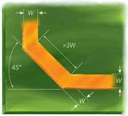
- Designers should use 45-degree bends as well as striplines (avoid microstrips) (Fig. 1).
- Avoid layer changes.
- Do not route any high-speed signals over slots.
- Use three-terminal capacitors to reduce inductive effects.
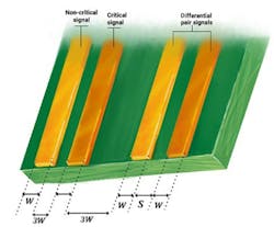
- Keep differential traces tightly spaced.
- Arrange all other traces spaced three trace widths apart from each other (Fig. 2).
Use EMI shielding
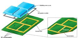
EMI can be minimized with the use of EMI shielding encasing a PC board (Fig. 3) and making use of shielded cables.
Spread-Spectrum Frequency Dithering
Texas Instruments’ TPS23730 Power over Ethernet (PoE) IC has a soft-stop feature that will lower any stress on the switching power FETs and ensure predictability of the shutdown procedure, while enabling reduced FET BOM cost. Programmable spread-spectrum frequency dithering (SSFD) is another excellent feature that will minimize the size and lower the cost of the EMI filter.4,10
This design also features a hiccup mode for overload protection when enabled, and ensures that the 802.3bt startup requirements are met.
On this front, believe it or not, actress Hedy Lamarr of the Silver Screen patented the “Secret Communication System” together with George Antheil in 1942. This frequency-switching system helped to improve the radio guidance of torpedoes. Fifty years later, in 1992, some researchers at Virginia Polytechnic in Blacksburg, Virginia, used the spread-spectrum technique in a power supply, as a method of spreading noise energy and reducing harmonic peaks that are associated with an SMPS.
Designers using the proper techniques for spread-spectrum technology, as outlined in Reference 4, can successfully apply those techniques to a system that will shape the noise signature while achieving a higher level of electromagnetic compatibility.
Dual Random Spread Spectrum (DRSS)
Spread-spectrum methods are typically used in switched-mode converters and controllers to reduce EMI from their switching mechanisms. Dual random spread spectrum (DRSS)8 employs a digital algorithm that’s able to spread spectral emissions in multiple frequency bands, while not trading off the performance between those bands.
Spread-spectrum methods, also known as dithering, can reduce EMI generated via fixed-frequency switching at the fundamental switching frequency, as well as its harmonics.
Summary
This article introduces some tried-and-true methods for reducing EMI, especially useful in switching power-supply designs. Filtering, shielding, and grounding are demonstrated. PCB design and layout must use solid EMI mitigation techniques for conducted and radiated EMI. And techniques such as DRSS and SSFD also help to reduce EMI.
References
1. “Conductive EMI Reduction Techniques for Soft-switched Half-bridge Buck Converters in Automotive Applications,” Weijie Han, Qi Cheng, Chen Chen, and Hoi Lee, 2022.
2. How to Reduce EMI to Improve Signal Integrity | Sierra Circuits (protoexpress.com).
3. Low EMI Noise Spreading in SMP.pdf.
4. Understanding Noise-Spreading Techniques and their Effects in Switch Mode Power Applications.
5. EMC Design Guidelines for Switched-Mode Power Supplies | System Analysis Blog | Cadence.
6. Design Techniques For Reducing EMI In SMPS Circuits.
7. PCB Design Techniques for Reducing EMI in Power Supplies - VSE.
8. EMI Reduction Technique, Dual Random Spread Spectrum.pdf.
9. EMI Reduction Techniques in Digitally Controllable Power Supplies - ScienceDirect.
10. Type 3 IEEE802.3bt-ready Active Clamp Forward Converter PoE Powered Device Reference Design.


