A New Generation of GaN Power ICs Mimic Silicon MOSFETs


Gallium nitride (GaN) is winning over the world of power electronics with its faster switching speeds and higher efficiency over that of silicon MOSFETs, which have dominated for decades. But nothing in the semiconductor industry comes easy.
Driving GaN power devices is a very complex and difficult process. The gate drivers used to control these power FETs must be specifically designed to ensure they can perform to the best of their ability reliably and safely. Cambridge GaN Devices (CGD), a power chip startup, is trying to reduce the difficulty level with a new family of e-mode GaN power FETs that it claims can be driven like a standard silicon MOSFET.
CGD said it’s able to eliminate the need for costly gate drivers, inefficient driving circuits, negative voltage supply rails, or additional voltage clamping components that can increase system complexity and cost.
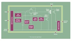
The GaN ICs are more than mere power FETs, the company told Electronic Design. They integrate lateral high-electron-mobility transistors (HEMT) with other building blocks, including protection, current sensing, and voltage regulation, in a single monolithic chip that improves reliability and robustness of the FET and the overall system. Using its ICeGaN technology, the startup said it upgraded the gate of the power device so it can be driven at up to 20 V, with a 3-V threshold voltage and turn-off voltage of 0 V.
CGD said ICeGaN underpins the company’s first-generation H1 family of 650-V GaN power ICs introduced in 2022 and its second-generation H2 family rolled out in 2023. They were both on display at APEC 2024.
The company faces a crowded field of competitors. Most of the movers and shakers in the power sector are investing in GaN power FETs, and many more companies are trying to tackle the difficulties of driving them. But the startup, founded in 2016 by CEO Giorgia Longobardi and CTO Florin Udrea after nearly a decade of research and development at Cambridge University, is confident that it’s filling an unmet need in the industry.
GaN: Switching Up the Field of Power Electronics
GaN is a wide-bandgap semiconductor (WBG) that’s been stirring up the field of power electronics in recent years. GaN power FETs are able to switch on and off up to 10X faster than silicon MOSFETs, giving them the ability to run at significantly faster slew rates (dv/dt).
Faster switching speeds mean the capacitors and other passives in the power supply—along with all of the inductors, transformers, and other magnetics interspersed with them—can be made proportionally lighter and more compact.

When GaN power FETs are turned on, the resistance between the source and the drain (RDS(on)) of the device turns out to be significantly less than that of a MOSFET. This translates into less power being uselessly expended during switching, making it possible to deliver more power in a smaller space as well as reduce heat. The presence of unnecessary heat means larger heatsinks or other forms of cooling, further adding weight and area.
But when GaN is engineered into a power FET, several tradeoffs surface. One of the peculiarities of GaN power FETs is that they operate in depletion mode (or d-mode), meaning that they are turned on by default, while silicon MOSFETs are normally off. This is a safety concern more than anything. The power transistors in switch-mode power supplies (SMPS) must be switched “off” to disconnect the input from the output when bias power is unavailable.
There are several ways to control the switching of GaN power devices so that they remain off. One possible configuration is to integrate a GaN power FET that is normally on with a silicon MOSFET that is normally off to control the GaN device’s switching. When the silicon MOSFET is turned off by the gate driver in the power system—located inside the same package as the power transistor or placed in front of it on the PCB—it outputs a negative voltage between the gate and the source of the GaN FET to keep it off.
Since the MOSFET in the system-in-package (SiP) is used to control turn-on and turn-off transitions, these GaN power FETs—also called “cascode”—tend to have very high robustness and reliability. Thus, they’re widely used to handle the larger amounts of power under the hood of electric vehicles or other heavy-duty systems that run at high voltages, high currents, or both, and encounter high electromagnetic interference (EMI) or other noise.
Besides the robustness and reliability at high power, these cascode FETs are also relatively easy to use. They can be paired with the same gate driver ICs currently used to control silicon MOSFETs and IGBTs.
But this comes with consequences. One of the most important features of GaN power FETs is the lack of a body diode, which removes reverse-recovery losses in hard-switching topologies. But indirectly driving the gate of the GaN power FET by driving the gate of the Si MOSFET throws a wrench into the works. These chips also have higher resistance. The resistance can also limit the maximum dv/dt of the GaN FET, resulting in high switching losses at heavy loads—and dulling one of the other advantages of GaN.
These cascode devices can also have a higher output capacitance (COSS), as the silicon MOSFET must apply a negative voltage to the gate of the GaN power FET before it switches off. COSS is one of the most important metrics in soft-switching topologies. Since these devices require a pair of power FETs, they’re also more vulnerable to parasitic inductance between the MOSFET and GaN FET in the package, which can limit performance.
Other companies are rearranging the internal architecture of the GaN power FET so that it’s turned off by default, the same as silicon MOSFETs. These enhancement-mode, or e-mode, FETs are all-in-one power ICs that bring improvements to gate charge (QG), output charge (QOSS), on-resistance (RDS(on)), and other figures of merit (FOM) to the table, unlocking faster switching frequencies and, thus, higher power density.
The tradeoff is that these GaN power FETs tend to be more susceptible to electromagnetic interference (EMI), and they can be permanently damaged by sudden high voltages stemming from high-voltage transients that occur during the switching of GaN power FETs. To operate at ultra-fast switching speeds, these power devices require the use of complex and expensive control and gate-driving circuits.
GaN Power ICs: All-in-One Power Conversion
To take full advantage of the more advanced power-handling properties of GaN power FETs, CGD is trying to split the difference between these approaches. The company said it specifically designed the gate of its e-mode GaN power devices to mimic the gate of a standard MOSFET that features a maximum voltage rating of 20 V, a 3-V threshold, and a 0-V turn-off voltage, making them relatively easy to use.
The gate of a MOSFET is a capacitor that must be sufficiently charged to turn “on” the power transistor, allowing the flow of current between the drain and the source of the FET. Removing the charge from the gate capacitor switches the FET “off.” The gate driver is used to supply enough current to the gate to handle the turn-on and turn-off. It must also apply a voltage higher than the threshold voltage, or the minimum voltage required to charge the FET’s gate.
If the voltage between the gate and the source of the power FET is lacking during the switching process—also called undershoot—it may not completely turn on or off, leading to higher resistance and power dissipation. On the other hand, excess voltage entering the power transistor's gate—also called overshoot—can permanently impair its performance. In most e-mode GaN power FETs, the turn-on voltage is relatively close to the maximum gate-to-source voltage (VGS), which tends to be around 7 V. That usually leaves a very small voltage margin.
Most GaN power FETs also operate at lower threshold voltages than silicon MOSFETs. This presents a problem because GaN power FETs must handle higher dv/dt during the switching process.
These transient voltages can inadvertently turn on the FET, resulting in shoot-through between the high- and low-voltage sides of the power supply, wasting unnecessary power. The startup said ICeGaN has a higher threshold voltage than other GaN power ICs in its class at 3 V, which means it can absorb higher dv/dt slopes and opens the door to faster switching speeds. The on-chip Miller clamp helps keep the power FET turned off without using additional negative voltage rails, CGD said.
The upshot is that the ICeGaN technology helps limit the risks of overshoot and undershoot. That also enables tighter control of the dead time between the turn-off and turn-on of the FET, improving efficiency.
Integration: The Future of the GaN Power FET?
CGD said ICeGaN adds several other building blocks vital to a modern power supply. The on-chip current-sensing and protection circuits can react in nanoseconds to short circuits and other overcurrent conditions to protect the power FET itself and the rest of the system from danger. By integrating current sensing, the power IC can be connected directly to ground, which helps draw away heat more effectively.

Intended for both soft- and hard-switching topologies, the company’s GaN power ICs add dv/dt control and incorporate a Kelvin pin for optimal high-frequency operation. In most switching power supplies, resistors between the gate driver’s output and the gate of the power device are used to control the slew rate (dv/dt) to bolster performance and reduce heat. This also allows adjustment of gate-loop ringing to minimize EMI.
On top of all that, the H2 family of GaN power ICs features another building block called NL3—short for “no load, light load”—that allows it to draw very small amounts of power when output current is at a minimum.
While it is bringing a good deal of innovation to the table, the startup is not alone in trying to tackle the difficulties of driving GaN power FETs. Various companies are trying to solve the problem, too, by driving the GaN power FET directly instead of indirectly through a standard MOSFET. Still others are integrating the gate driver in the same package as the FET to reduce complexity and power surrendered to parasitics in the PCB, while many more are pushing out more advanced gate-driver ICs for GaN FETs.
Though it’s facing competition from many of the leading players in the world of power semiconductors as well as several other startups, CGD said it’s confident in its chances. The company is targeting its 650-V GaN power ICs at everything from chargers and adapters for PCs and other consumer electronics that start out at around 65 W to power inverters for solar, wind, and other forms of renewable energy range up to 3 kW.
Further out, as AI processors drive up the power demands of data centers, the startup plans to upgrade its technology for use in power-supply units that can output tens of thousands of watts at a time. As Longobardi pointed out, “With data centers now demanding 100 kW per rack and [companies] predicting even more in the very near future, power system designers are looking to employ GaN devices in new architectures.”
Check out more of our coverage of APEC 2024. Also read more articles in the TechXchange: Gallium Nitride (GaN).
About the Author

James Morra
Senior Editor
James Morra is the senior editor for Electronic Design, covering the semiconductor industry and new technology trends, with a focus on power electronics and power management. He also reports on the business behind electrical engineering, including the electronics supply chain. He joined Electronic Design in 2015 and is based in Chicago, Illinois.
Comment About the Article
To join the conversation, and become an exclusive member of Electronic Design, create an account today!

Leaders relevant to this article: