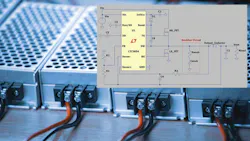
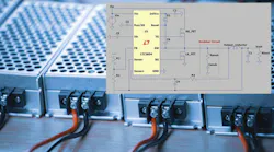
Use Snubber Circuits to Dampen Noise in DC-DC Converters
What you'll learn:
- Understand how parasitic inductance and capacitance create switching-node ringing and EMI in DC-DC converters.
- Learn how RC snubber circuits reduce voltage overshoot, ringing, and EMI in synchronous buck regulators.
- See how to calculate, simulate, and optimize snubber values while balancing noise reduction and efficiency.
Power designers are constantly pursuing DC-DC converter designs with higher efficiency and smaller sizes. These gains are often achieved by using faster switching frequencies to shrink inductors and capacitors in the solution.
However, that also increases the impact of parasitics, which are unintended inductances and capacitances emanating from PCB traces and power FETs themselves. At fast switching speeds, interaction with these parasitics can cause significant voltage overshoot and ringing at the switching (SW) node.
This ringing not only places additional voltage stress on the FETs, but it also causes unwanted electromagnetic interference (EMI). EMI disrupts the performance of a system through electromagnetic induction, electrostatic coupling, or conduction. It’s a critical design challenge in industries like automotive, medical, and test and measurement, where meeting strict EMI standards is crucial for product certification and time-to-market.
Reducing ringing and other noise is often left until late in the design cycle, making it difficult to resolve. Using low-noise DC-DC regulators or fine-tuning the placement of power electronics on the PCB can help with that. But another approach — the snubber circuit — can effectively mitigate noise if those initial steps weren’t taken.
Taking a synchronous buck regulator as an example, this article introduces the problems associated with switching ringing before explaining how to design and optimize a snubber to dampen it. Using LTspice and typical parasitic models, we will simulate the ringing seen on a standard PCB and demonstrate the impact of the calculated snubber values on both the ringing and the overall efficiency.
Where, When, and Why: Understanding Parasitics
In a buck converter, voltage overshoot and ringing at the switching node are a direct result of high speeds. These fast-switching frequencies interact with the parasitic inductances and capacitances in the circuit. Such parasitics are formed by copper traces in the PCB and the components themselves, particularly the power FETs.
>>Download the PDF of this article, and check out the TechXchange for similarly themed articles and videos

Essentially, the stray inductance from the PCB traces and the FET package forms an LC tank circuit with the FET’s parasitic output capacitance (COSS). This makes both PCB layout and the selection of the MOSFET critical factors in power-converter designs.
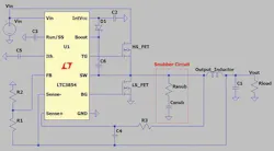
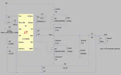
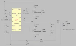
The magnitude of stray inductance varies from one design to another. But for the purposes of the simulations below, a value of 5 nH around the FETs is a reasonable starting point. This value can be significantly higher with a poor layout, as inductance values can reach up to 10 nH for every 25 mm of trace length. Figure 1 highlights a typical power-controller circuit using the LTC3854, with the expected parasitics shown in red.
What’s a Snubber Circuit and How Does It Work?
After identifying the switching noise and the parasitic elements that contribute to it, the next step is damping it. A snubber circuit — typically a series resistor-capacitor (RC) network — is commonly used to absorb the voltage spikes and ringing that appear at the SW node.
A snubber works by providing a controlled outlet for high-frequency energy from the parasitic LC tank. When the switch turns off, the snubber capacitor begins to charge, absorbing energy that would otherwise cause ringing. The snubber resistor then dissipates this stored energy as heat, effectively damping the oscillations.
By introducing a new resonant frequency and adding resistance to the circuit, the snubber reduces the peak voltage and duration of the ringing, protecting the power switches from overvoltage stress.
Figure 2 shows a typical buck converter with the snubber circuit positioned from SW node to ground (GND) as close as possible to the MOSFET.
The Snubbing Power of a Snubber Circuit
One of the keys to designing a snubber is determining the optimal resistance and capacitance values for the RC network used to damp voltage ringing and reduce EMI in switching circuits. The process involves finding the parasitic inductance and capacitance of the switching circuit (through simulations or using an oscilloscope for actual hardware) to measure ring frequency and then calculating the snubber’s characteristics from there. Here are the most important steps:
1. First, measure the ringing frequency of the switching node. This will be the peak of the first spike to the peak of the second spike. As a reminder, when measuring the parasitics on physical hardware with an oscilloscope, bandwidth limiting must be turned off. Also, a short scope ground must be used to ensure the ringing is visible.
2. Add a capacitance from SW to GND such that it reduces the ringing frequency (fr) by approximately half the measured value above. Experiment with some different capacitance values here.
3. This will give the parasitic capacitance (CP) by dividing that added capacitance by 3.
4. Knowing the parasitic capacitance, the parasitic inductance (LP) can be calculated by:
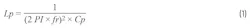
The characteristic impedance is calculated by:
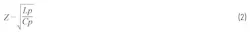
To attenuate the ringing, it will be necessary to use a snubber resistor that’s approximately equal to the impedance calculated in Equation 2, generally a few ohms:

The capacitance value should then be selected by taking the CP value calculated in Equation 3 and increasing it by a factor of 1X to 4X higher.
Simulating and Analyzing a Snubber Circuit in LTspice
Having established the fundamentals of noise generation, measurement techniques, and initial snubber value calculations, the next step is to simulate these effects. This section uses LTspice to illustrate the impact of PCB parasitics on ringing and overshoot in the switching node, as well as the effectiveness of a snubber circuit in mitigating these effects. The following analysis will be conducted to compare the buck converter’s operation with and without a snubber:
1. Modeling parasitics: First, a model is created that includes the parasitic elements to show the ringing and overshoot at the SW node without any snubber.
2. Initial snubber impact: The circuit is subsequently evaluated using the initially calculated snubber values to show the resulting reduction in ringing amplitude and overshoot.
3. Snubber optimization: Then, the component values of the snubber circuit are adjusted to achieve the optimal balance between ringing suppression and minimal power dissipation
4. Efficiency analysis: Finally, compare the overall efficiency of the buck converter both with and without the optimized snubber to quantify its impact.
Modeling Parasitics and Measuring Ringing
The LTC3854 synchronous buck controller helps highlight how poor PCB layout can introduce significant parasitic effects that lead to switch-node ringing. The device uses external power FETs, so the influence of layout parasitics becomes pronounced.
In this simulation, the effects of a poor layout are modeled by adding a 5-nH parasitic inductance — a realistic value considering that approximately 25 mm of PCB trace can contribute 10 nH or more of inductance.
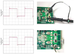
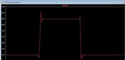
Before calculating the snubber values, it’s essential to understand the extent of this problem. This is typically done by monitoring the SW node with an oscilloscope. To capture the rising voltage waveform accurately, configure the volts per division to accommodate the full voltage range (0 V to VIN) and adjust the time base to view a single transition.
Crucially, a proper probing technique is essential for accurate measurement. A common mistake is using the long ground lead of the oscilloscope probe, which introduces its own parasitic inductance. This inductance can cause artificial ringing on the measurement, giving a misleading representation of the actual switching activity. It’s critical to replace the long lead with a short ground spring to reduce the loop inductance and improve measurement fidelity.
The images in Figure 3 illustrate the dramatic difference in measurement results. It demonstrates how a long ground lead can artificially introduce significant overshoot and ringing, leading to a misdiagnosis of the circuit’s performance.
Un-snubbed Simulation Results
The different parasitic inductances and capacitances modeled in the buck converter are outlined in Figure 4, while Figure 5 illustrates the impact of these parasitics on the profile of the switching node. The LC tank formed by these elements causes significant overshoot and ringing.
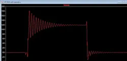
As the simulation shows, the voltage peaks at just over 18 V, which is significantly higher than the expected 12 V. This overshoot is a major concern, as it can exceed the absolute maximum voltage ratings of the MOSFET, potentially damaging the component or reducing its long-term reliability. The ringing is also problematic, as it indicates the MOSFET isn’t operating in its clearly defined on-off states.
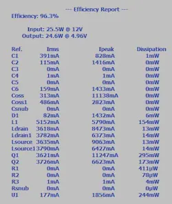
The overall efficiency of the circuit is 96.3%, which seems high at first glance (Fig. 6). However, note that this efficiency is without a snubber. The following sections will show how adding a snubber, while crucial for mitigating ringing, will have a small, quantifiable impact on this efficiency.
Parasitic Model and Snubber Not Calculated
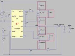
Figure 7 shows the same schematic as Figure 4, but with a simple RC snubber included from the switching node to ground. Note that this is a guessed starting snubber value and hasn’t yet been calculated, so it will not be optimal.
In Figure 8, the resulting switching node waveform is highlighted, and it’s been significantly improved. The peak overshoot is approximately 4 V lower at 14 V, and the oscillation seen after turn-on has been significantly reduced.
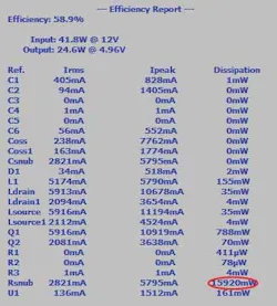
However, the efficiency has been reduced significantly to 58.9%, with the majority of the loss associated with the snubber resistor (Fig. 9). This shows that while an unoptimized snubber can mitigate ringing, it can also drastically reduce efficiency.
Streamlining Snubber Circuits
When it comes to optimizing a snubber circuit, the goal is to select an RC snubber that effectively dampens the ringing without causing excessive power loss.
First, determine the parasitic LC components of the circuit. The initial simulation (without a snubber) showed a ringing frequency of 23.41 MHz. Then, add a known capacitor from the SW node to ground to observe the change in the ringing frequency. A new simulation with a 14,000-pF capacitor at the SW node reduces the ringing frequency to 12 MHz.
Using the resonant frequency formula fo = 1/(2 × PI√LC) can determine the parasitic capacitance. The change in frequency is caused by the increase in total capacitance. The new total capacitance (Ctotal) is:
Ctotal = Cparasitic + Cadded
The relationship between the original frequency (fold) and the new frequency (fnew) is:

Solving for Cparasitic:
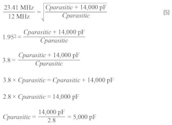
This indicates that the circuit has a parasitic capacitance of approximately 5,000 pF. With the parasitic capacitance, the parasitic inductance can be calculated:
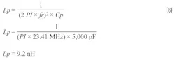
The impedance of the circuit is calculated by:
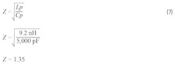
The snubber resistance is set to be greater than the characteristic impedance noted above; in this case, a standard value of 1.5 Ω.
Next, the snubber capacitance, Csnubber, is typically sized to be at least equal to the parasitic capacitance, up to 4X this value. For the initial simulation, use a value that’s double the parasitic capacitance to ensure sufficient energy absorption, setting Csnubber = 2 × Cparasitic = 2 × 5,000 pF = 10,000 pF. With the optimized snubber resistance and capacitance, plug these values back into the LTspice simulation to see how the circuit performs.
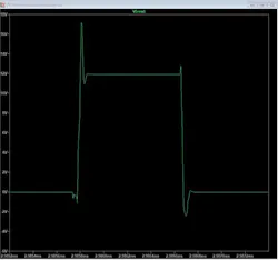
Figure 10 shows the resulting waveform with a 1.5 Ω + 10,000 pF snubber network. The ringing has been significantly dampened, as intended by the optimized design. The overshoot has also been reduced from more than 18 V to 17.2 V with these calculated snubber values. While some overshoot remains, the result highlights the inherent tradeoff in snubber design: Perfectly eliminating all overshoot and ringing often requires snubber values that result in greater power loss and reduced efficiency.
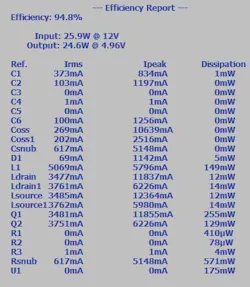
Furthermore, the overall efficiency is now 94.8%, which is a significant improvement over the 58.9% seen with the uncalculated snubber (Fig. 11). There will always be some efficiency impact with a snubber, as the resistor dissipates a small amount of power. However, by optimizing the component values based on the parasitic LC tank, the impact on efficiency can be minimized.
Tackling the Complexities of Snubber Circuits
Understanding and mitigating switching node ringing is a critical step in designing a reliable switching regulator. As shown, this high frequency noise isn’t an inherent flaw, but a direct consequence of the parasitic LC tank formed by PCB trace inductance and the switching components’ capacitance.
By taking a methodical approach — accurately simulating the undamped ringing frequency and associated voltage overshoot — the problem can be demystified. This allows for calculating a precise snubber network value, where the resistor critically damps the circuit by matching the parasitic impedance, and the capacitor acts as an energy sink.
The simulation examples clearly demonstrate that a well-designed snubber is an elegant and effective solution. It trades a small, manageable power loss for a significant improvement in both EMI performance and system reliability. Ultimately, incorporating this simple but powerful RC network can quickly transform a noisy and potentially vulnerable power supply into a clean and dependable one, ensuring the longevity and compliance of the final product.
Reference
Ballar, Wesley and Jacob Ciolfi. “Lab Skills for Switch-Mode Power Supply Evaluation—Part 1: Measuring Voltage Ripple and Switching Node.” Analog Dialogue, Vol. 59, January 2025.
>>Download the PDF of this article, and check out the TechXchange for similarly themed articles and videos
About the Author

Diarmúid Carey
Principal Engineer, European Centralized Applications Center, Analog Devices Inc.
Diarmúid Carey is a principal engineer with the European Centralized Applications Center at Analog Devices. Based in Limerick, Ireland, he has worked as an applications engineer since 2008. Diarmúid joined Analog Devices in 2017, providing design support for the power and isolation portfolio for European broad-market customers. He holds a Bachelor of Engineering degree in computer engineering from the University of Limerick.
Comment About the Article
To join the conversation, and become an exclusive member of Electronic Design, create an account today!

Leaders relevant to this article: