The eGaN FET-Silicon Power Shoot-Out: 2: Drivers, Layout
Find a downloadable version of this story in pdf format at the end of the story.
To determine the gate drive circuit requirements, and how they differ from traditional silicon MOSFET drivers, it is necessary to compare silicon against eGaN FET device parameters (Table 1). When considering gate drive requirements the three most important parameters for eGaN FETs are:
- Maximum allowable gate voltage
- Gate threshold voltage
- “Body diode” voltage drop.
The maximum allowable gate-source voltage of 6 V{2} is low compared with traditional silicon. Second, the gate threshold is also low compared to most power MOSFETs, but does not suffer from as strong a negative temperature coefficient. Third, the “body diode” forward drop can be a volt higher than comparable silicon MOSFETs.
GATE PULL-DOWN RESISTANCE
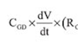
A great advantage offered by eGaN FETs is the possible switching speed. However, the higher di/dt and dV/dt that accompany this new capability not only require a layout with less parasitic capacitance, resistance, and inductance, but also cause some new considerations for the gate driver. Let's consider a half- bridge with a high dV/dt turn-on of a complementary device as shown in Fig. 1. The ‘Miller’ charge current flows from the drain (switching node) through CGD and CGS to the source as well as through CGD to RG (internal gate resistance) and RSink (gate driver sink resistance) to the source. The requirement for avoiding dV/dt (Miller) turn-on of this device is given by:
Where:
α = Passive network time constant (RG + RSink) × (CGD + CGS)
dt = dV/dt switching time
Thus, to avoid Miller turn-on of an eGaN FET, it is necessary to limit the total resistance path (internal gate resistance RG and external gate drive sink resistance RSink) between the device gate and its source. One can argue that, for devices with good Miller ratios (QGD/QGS(VTH) < 1), this is not required. Practically, since QGD increases with VD, this ratio will slowly worsen with increasing switching voltage and canít solely be relied on to prevent Miller turn-on.
By the same token, Equation (1) does not need to be adhered to at very low bus voltages where QGD/QGS(VTH) is still much less than one. To be safe, a gate drive pull-down resistance of 0.5 Ω or less is recommended for higher voltage devices.
GATE PULL-UP RESISTANCE
Because the total Miller charge (QGD) is much lower for an eGaN FET than for a similar on-resistance power MOSFET, it is possible to turn on the device much faster. As stated above, too high of a dV/dt can actually reduce efficiency by creating shoot-through during the “hard” switching transition. It would therefore be advisable to have the ability to adjust the gate drive pull-up resistance to minimize transition time without inducing other unwanted loss mechanisms. This also allows adjustment of the switch node voltage overshoot and ringing for improved EMI. In power MOSFET applications, this is achieved by placing a resistor and anti-parallel diode in series with the gate drive output. For eGaN FETs, however, where the threshold voltage is low, this is not recommended. The simplest general solution is to split the gate pull-up and pull-down connections in driver and allow the insertion of a discrete resistor as needed.
Continue on next page
The eGaN FET reverse bias or “body diode” operation has the benefit of no reverse-recovery losses. This advantage, however, can be offset by the higher “body diode” forward voltage drop2. The diode conduction losses can therefore be significant, especially at low voltages and high frequencies. However, unlike diode reverse recovery losses; these conduction losses can be minimized through proper dead-time management that minimizes the “body diode” conduction interval.
Silicon gate drivers and controllers tend to have an effective minimum dead-time around 20 ns (±10 ns) for low voltages, and it increases with bus voltage to around 400 ns (±100 ns) for 600 V drivers. With eGaN FETs, both the gate capacitance and Miller capacitance are significantly lower than equivalent silicon devices, leading to smaller turn-on and turn-off delays as well as shorter switching times. These shorter and less variable switching times allow for much tighter dead-time control which, in turn, would be beneficial in reducing “body diode” conduction loss. A reduction of dead-time between half and one-fourth the above values, with a similar reduction in the variation, would be preferred. In the interim, it would be beneficial for an eGaN FET gate driver to have dead-time adjustment. This can be done simply by either lengthening the pulse by delaying turn-off, or shortening the pulse through delaying the turn-on, depending on the gate drive source.
GATE DRIVE SUPPLY REGULATION
The current maximum gate voltage limitation of 6 V on the eGaN FET does add restrictions to the gate drive supply range, and requires at least some form of supply regulation. Of greatest concern is the floating or high-side supply in a half-bridge configuration. A simple implementation to improve matching between low-side (ground referenced) and high-side supplies is through the use of a “matching” diode as shown for a discrete gate drive implementation in Fig. 2.
This implementation is only suited for complementary switched, half-bridge applications where the dead-time and “body diode” conduction is minimal. For applications where the eGaN body diode conduction can be significantly longer than the bootstrap diode turn-on time, the ~2 V “body diode” voltage drop will add to the supply voltage and can cause overvoltage of the high-side supply. In such cases, some form of post bootstrap supply regulation is required. Thus the limited overdrive headroom of eGaN FET does increase the gate drive supply complexity when compared to silicon.
Given the information on how the eGaN FET drive requirements differ from power MOSFETs, it is possible to define an eGaN FET gate driver IC. At first, to leverage the existing MOSFET controller and level-shifter infrastructure, a simple eGaN FET driver interface IC is suggested. This part is defined to interface between any controller and the eGaN FET as shown in Fig. 3. The same part could also be used for synchronous rectification and single switch isolated topologies (such as flyback and forward). These would also be suited for digital controllers where the gate drive function would normally be external to the controller anyway. The suggested device pin-out and pin descriptions are given in Fig. 4 and Table 2, respectively.
LAYOUT CONSIDERATIONS
The maximum allowable gate voltage of 6 V is only one volt above the recommended 5 V drive voltage. This limited headroom requires an accurate gate drive supply, as well as a limited inductance between the eGaN device and gate driver as the inductance can cause a voltage overshoot on the gate. Although some overshoot is acceptable, overshoot can be avoided entirely if the gate inductance is limited to:
Continue on next page
Where:
RSource = Source resistance on the gate driver
LG = Loop inductance between the gate driver and eGaN device
Thus, for a given gate loop inductance there will be a minimum source resistance value to keep VGS from exceeding its maximum limit.
With the EPC devices being chipscale packages with negligible package inductance, the question of common source inductance could be considered a layout issue rather than a gate driver requirement. These aspects, however, are much more intertwined to draw such a sharp distinction. The addition of CSI (common source inductance) effectively reduces efficiency by inducing a voltage across the CSI during di/dt that opposes the gate drive voltage, thus increasing turn-on and turn-off times. It is therefore critical to minimize common source inductance for optimum switching performance. In what seems to be at first glance contradictory, the increase of CSI will decrease the possibility of Miller turn-on{3} if one accepts the cost of increased switching loss that it entails. This is due to the fact that at the “hard” turn-on of the complementary device, the current commutation di/dt across the CSI induces a negative voltage across the gate to help keep the device off during part of the voltage transition. What is not stated is that the CSI, gate capacitance, and gate drive pull down loop now forms an LCR resonant tank that needs to be damped to avoid an equivalent positive voltage ringing across the gate. This ringing could turn the device on again near the end, or even past the end of the voltage transition. Although increasing the gate drive sink resistance can help damp this LCR resonance at the cost of increased Miller turn-on sensitivity, the addition of a ferrite bead that is resistive (lossy) at the resonant frequency can achieve the same result with less increase in Miller turn-on sensitivity. Please refer to Fig. 5 for the equivalent circuit and Fig. 6 for conceptual switching waveforms. This effect may sometimes be hard to distinguish from dV/dt induced Miller turn-on. In short, CSI is much more important to eGaN FETs than silicon, due to the higher di/dt and dV/dt and should be minimized as much as possible through careful layout.
SUGGESTED LAYOUTS
Given the different considerations listed above, it is possible to develop some recommended layouts. The layouts presented depict a half-bridge configuration, but following the above requirements can be expanded for other applications as well.
Simple, as well as complex four layer PCBs are presented in Figs. 7 and 8, respectively. It should be noted that the copper thickness needs to be maximized to limit resistive losses and improve thermal spreading (2 oz copper on outer layers is recommended). In both of these layout examples, the source connection of each part is brought underneath it to act as shield and minimize additional parasitic CGD. In the simpler layout (Fig. 7) the gate return connection is made on the smaller source pad to separate gate return current and device drain current paths in the source, thus minimizing CSI.
In the more complex design in Fig. 8., this is taken further by connecting every source connection through Layer Two to the shield that now doubles as the gate drive return path. Drain connections are brought out similarly on the third layer. The trade-off here is that to achieve a much lower CSI and overall loop / layout inductance, the geometry requires increased parasitic capacitance - in particular CDS (output capacitance) - as there is still the need to minimize the parasitic gate to drain capacitance.
Continue on next page
THERMAL CONSIDERATIONS
Due to the fundamentally lower eGaN on-resistance{4}, these devices are only a fraction of the size of an equivalent on-resistance power MOSFET die, and therefore have a much higher equivalent thermal resistance. However, eGaN FETs also have a much lower FOM1 and will therefore have offsetting lower switching power losses.
Can this improvement in power loss make up for the higher thermal resistance?
In order to answer this question we need to look at two common scenarios; (1) devices mounted as “flip chips” on a printed circuit board without additional heatsinking, and (2) devices mounted with dual-sided cooling.
Because eGaN FETs are constructed on a very thin layer of heterojunction material on top of a standard silicon wafer {4}, devices mounted directly onto PCBs without any backside cooling behave thermally like any similarly mounted silicon device. The variables needed to completely understand the resulting thermal performance are, (1) PCB copper area, (2) Copper thickness, (3) PCB material, and (4) airflow over the device.
Reference[6] tests several industry standard packages mounted directly onto FR-4 PCB material. Measurements were made on one square inch, 2-ounce Cu, and on devices with only enough Cu to make electrical contact to the leads. This methodology separated the effect of device footprint from the cooling that comes from the copper on the PCB. Relatively little impact was seen when different packages were mounted on one square inch Cu (the minimum RTHJA was 18°C/W for a D2PAK and the maximum was 34°C/W for an SO-8) because the dominant thermal resistance factor was the heat dissipating through the PCB. Consistent with these tests, EPC estimates that RTHJA for eGaN FETs mounted to one square inch of 2 ounce Cu should be about 40°C/W in still air {5,7}. This performance can be improved significantly with increased airflow.
DOUBLE-SIDED COOLING
In order to determine the best possible top-side cooling for EPC's eGaN FETs, the setup in Fig. 9 was constructed. RDS(ON) was used as the temperature sensitive parameter and the heatsink was water cooled for these “best-case” thermal measurements. Across the family of EPCís eGaN FETs, the data suggests a 12-14°C-mm2 normalized RTHJA when cooling is primarily through the silicon substrate beneath the eGaN FET active area. Under these conditions, EPC's large area eGaN FETs have an RTHJC of about 2°C/W and the small area FETs have an RTHJA of about 8°C/W.
Practical implementations of double-sided cooling are certainly less elaborate than the one shown in Fig. 9, and result in higher final thermal impedance. Fig. 10 illlustrates a configuration where two devices are simultaneously cooled by one heat sink. Here, multiple die is placed under the same heatsink; however, care must be taken to avoid mechanical damage from uneven pressure on die that might be slightly tilted or at different heights off the PCB. Thermally conductive materials such as from 3M{8}, Dow Corning {9}, or Bergquist {10} have been successfully used to double-side cool multiple die under one heatsink.
To realize full advantage from EPC's eGaN FETs, designers must understand how to design cost-effective drive circuitry that works on a cost-effective PCB. In this installment, we looked at gate drive requirements, layout, and thermal design considerations designers must consider to develop products that leverage eGaN FET advantages.
In our next chapter, we will demonstrate an eGaN FET-based Power Over Ethernet (POE) design that has greater power density than similar circuits using state-of-the-art power MOSFETs.
REFERENCES:
-
powerelectronics.com/power_semiconductors/power_mosfets/fom-useful-method-compare-201009/
-
EPC datasheet of EPC1001. epc-co.com/epc/documents/datasheets/EPC1001_datasheet_final.pdf
-
Fairchild Semiconductor AN-7019, “Limiting Cross-Conduction Current in Synchronous Buck Converter Designs”, www.fairchildsemi.com/an/AN/AN-7019.pdf#page=1
-
EPC article, “Fundamentals of Gallium Nitride Power Transistors”, epc-co.com/epc/documents/product-training/Appnote_GaNfundamentals.pdf
-
International Rectifier, whitepaper, “A New Generation of Wafer Level Packaged HEXFET Devices” www.irf.com/technical-info/whitepaper/pcimflipfet.pdf
-
International Rectifier, www.irf.com/technical-info/whitepaper/thermalpcim02.pdf
-
EPC article, “Using Enhancement Mode GaN-on-Silicon Power Transistors”, epc-co.com/epc/documents/product-training/Using_GaN_r4.pdf
-
Dow Corning Pads: www.dowcorning.com/content/etronics/etronicspadsfilm/
-
Bergquist Pads: /www.bergquistcompany.com/thermal_materials/gap_pad/pdfs/gap-pad-vo-soft/PDS_GP_VOS_12.08_E.pdf
Download the story in pdf format here.
Comment About the Article
To join the conversation, and become an exclusive member of Electronic Design, create an account today!

Leaders relevant to this article: