Here�s what test engineers charged with production-level device testing need to know when specifying mixed-signal SOC test systems.
Every semiconductor manufacturer faces continuing pressure to reduce manufacturing costs because of constant demands to lower the average selling price of devices. Although semiconductor manufacturers currently are seeing improvements in their revenues with a substantial increase in device volume, product margins continue to be under significant pressure.
As a result, semiconductor manufacturers must analyze their system-on-a-chip (SOC) device test strategy at wafer and final test. It is not unusual to model the cost components of the production line. SOC wafer and final test are modeled at a cost of only 2% to 4% of the total product�s revenue. Also, mixed-signal SOC device test strategies involving structural and functional test have been developed and deployed to help achieve a low test cost.
But in the end, one of the biggest impacts on overall test cost is device throughput. To have the greatest impact on throughput, manufacturers of mixed-signal SOCs are turning to multisite testing. To attain the high-throughput benefits, multisite test should be implemented early in production rather than starting with a single-site test program and later adapting it for multisite test. In addition, the test-time efficiency of the multisite test program vs. the single site is key to attaining optimal cost-of-test benefits.
The efficiency of multisite testing in relation to the time required to test one device in a single site is defined as
Efficiency = ?t / ?n
t1
where: ?t = change in total test time
?n = change in number of sites
t1 = time to test one device in a single site
If, for example, t1 = 2 s and 10 sites are used to achieve a total test time of 15 s, or 1.5 s/device, then the efficiency of this multisite example is 1 – 13/9/2 = 27.7%. If the average test time had been reduced to 0.5 s by the addition of nine sites, the efficiency would have been 1 – 3/9/2 = 83.3%. Taking the definition to the extreme, 100% efficiency means that no additional test time is required to test devices at additional sites.
Today�s Devices
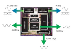
Today�s devices present a broad range of pure analog and pure digital, with everything in between considered mixed signal, a mix of analog and digital content used in a broad range of end-use markets. To create a device, semiconductor manufacturers typically incorporate reusable IP cores or functional blocks. These cores are combined to construct an SOC (Figure 1).
Most of the digital IP cores come with a set of structural test vectors, which may be scan-based vectors, or with built-in self-test (BIST) features as used for embedded memories. The building blocks in the device can be tested using structural test. With structural test, each of the cores in the system is tested, but the interoperability among the different cores is not tested.
Structural test does not test the device as a system. Because mixed-signal cores may not have structural test capability available and because the interoperability of the device cores must be tested to validate that the device works as a system, functional testing is required as well. Functional testing is used to test the device�s capability to meet specifications when replicating its operating environment.
Mixed-Signal SOC Testing
As shown in Figure 1, the blocks of a mixed-signal SOC device often are running at unique frequencies that are not necessarily multiples of each other. In this example, each block has a different frequency associated with it. A stand-ard video frequency is 14.318 MHz. The audio converters are running at the standard sampling rate of 96 kHz. The serial bus interface operates at 1,600 Mb/s and the DDR interface at 266 MHz.
When simulating the operating environment, the tester must generate multiple time domains, whether pure digital, mixed-signal, or analog time domains.
Mixed-signal SOC devices generate a great deal of data simultaneously. On the video converter side, there might be three different converters, each producing data at the same time. For example, there could be anywhere from two to five audio converters if the device is supporting surround-sound capability. There is a great deal of data pouring out of the chip as well as the data that needs to go into it.
In the functional test environment, all the data must be analyzed and processed simultaneously to determine the performance and functionality of the mixed-signal blocks. The objective is to achieve test speed that�s limited only by the operation of the device. This can be accomplished by a test-system architecture that precisely controls instrumentation in device clock time.
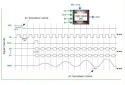
Consider the high-speed digital-to-analog converter (DAC) test example shown in Figure 2. The device has VCC input with a series of digital pins, a clock pin, and a synchronization pin to indicate when to start converting data. There is an 8-b parallel word as the data input. The output of the DAC is an analog output called Aout. The example shows the digital pattern and the analog event that takes place during test.
To perform the test in this example, the VCC voltage level needs to change to 4.5 V as required by the test specification. The digital test pattern that drives the device clock and data also can initiate instrument setup and control. This capability allows the pattern to change the DC instrument to 4.5 V and settle for a specified number of device clock cycles.
In Figure 2, the very first vector sends a command to the DC instrument to change its voltage. The next device vector is repeated 100 times to allow the device to settle to the new voltage. At that point, the digital representation of the analog signal is input on the parallel 8-b port. In the tester code, that�s indicated by the START command, which tells the digital signal generator to start sending data.
Precisely 10 device clock cycles later, the digitizer is triggered to capture the analog signal on pin Aout. This is controlled by the digital pattern telling the digitizer to trigger and capture the analog signal coming out of the device. The test-system computer is not involved in the timing of these instrumentation events.
The instruments are controlled in device clock time by the digital pattern. This capability enables testing at device speed. This precise sequence of events will occur each time the device program is run, guaranteeing repeatability of the test measurement.
Solutions for Multisite Testing
To thoroughly address high-efficiency multisite test for mixed-signal SOC, both the tester hardware and software must be designed for multisite test from the ground up. Multisite solutions cannot be software-only solutions that are added to the system.
The hardware and software must be integrated to handle management of functions such as the setup and control of test instrumentation in parallel. To ensure complete parallelism, system resources cannot be shared. Instead, the system must be expandable to handle high-density instruments.
Scalability of a test system is critical to optimize multisite efficiency. Efficiency will be optimized by avoiding the use of shared tester resources.
This means that dedicated power supplies, V/Is, arbitrary waveform generators, digitizers, and digital channels must be available to each device test site. The test-system platform needs the flexibility to add instruments easily.
The instrument cards must be high density, effectively reducing the number of instrument cards needed in the tester. For that reason, the electrical interconnects and mechanical structure required to support the instruments are reduced.
Computer Bus Communications To the Instruments
The test-system software and hardware must be implemented in a manner where the computer only sends one command across the computer bus and each instrument connected to a device test site listens and responds to the command.
This approach not only reduces the computer bus I/Os, but also allows the instruments to settle in parallel. This will optimize the throughput of the multisite program by eliminating added overhead because of additional sites, maintaining high efficiency no matter how many test sites are involved.
Availability of Time Domains
Device cores in new mixed-signal SOC devices can operate at a variety of noninteger-related frequencies. In some cases, it is necessary to synchronize the tester to a time domain produced by the device, aligning the pattern in the tester�s digital instrument to a data sequence or digital edge from the device. This can be accomplished with capabilities such as match mode and edge find.
The tester must have an additional time domain for each device test site to allow each site�s digital pattern to synchronize to each device in parallel. Without the extra time domain per site, synchronization would occur serially, reducing the overall efficiency of multisite testing.
DSP for Device Data
Mixed-signal device testing has adopted the use of DSP techniques to obtain a set of test measurements from large data sets. When moving to multisite testing, the amount of data increases by a factor equivalent to the number of sites being tested.
Three primary actions need to take place: capture the data, move the data to the processor engine, and then calculate the results. At each of these steps, parallelism of resources and a streamlined data flow are needed to attain the best efficiency.
The instrument that is capturing the data samples determines when the data should be moved. This removes any overhead associated with the computer polling each of the instruments to determine when they are done capturing data. Once the instrument has completed the data capture, it moves the data via dedicated buses to a set of dedicated processing engines. Using dedicated buses and a set of general-purpose processors eliminates the bottlenecks of conventional shared computer bus architectures and places the entire DSP function into the background of the testing activity.
Test-Program Development Environment
With short product life cycles for mixed-signal devices, test-program development time becomes critical. If it takes several months to develop the multisite test program from the single-site program, the production ramp could be missed. The software and hardware need to make this transition simple and fast to have the test program in place before the production ramp occurs.
To accomplish this, the programming environment must assume that the device will be tested on a multisite system. As instrument setup commands are written for one site, the software needs to assume that other sites will perform the same operation. The software also must manage situations where a shared tester resource may need to be used across the sites.
The test programmer needs to easily indicate which resources are shared, and the test-program environment should manage this automatically in the background as a serial portion of the test flow. Although this does impact the test time and efficiency, it enables easy implementation of the multisite test program when not all instruments are replicated from site to site.
The debug environment must allow the user to focus on the activities at a specific site as well as view data and test results at the other sites. These kinds of features must be embedded in the operating software to ensure rapid generation and debug of the multisite test program.
Summary
A system for multisite test that is designed from the ground up with integrated hardware and software elements can provide semiconductor manufacturers with an easy-to-use, highly efficient, low-cost multisite test solution. With the complete test cell analyzed for the maximum number of effective sites, efficient mixed-signal multisite throughput will be achieved, providing the lowest cost-of-test solution.
About the Author
Randy Kramer is the technical marketing manager for the Semiconductor Test Division at Teradyne. The 22-year veteran of the ATE industry has a background in mixed-signal testing and graduated from Rensselaer Polytechnic Institute with a B.S.E.E. Teradyne, 321 Harrison Ave., Boston, MA 02118, 617-422-2700,
e-mail: [email protected]
July 2004
About the Author
Voice Your Opinion!
To join the conversation, and become an exclusive member of Electronic Design, create an account today!

Leaders relevant to this article:


