Members can download this article in PDF format.
What you’ll learn:
- The basic considerations when choosing a timing solution for today’s technologies.
- The difference between a crystal oscillator and an integrated clock device.
- Use cases and performance factors for crystal oscillators and integrated clock devices.
As technology has become more digital, timing systems have become a critical component in most electronic systems. Smartphones, PCs, IoT devices, networking equipment, and many other devices rely on internal timers, counters, and clocks. These timing components generate timing pulses that enable the internal electronics to synchronize events with a precise frequency, ensuring data transmission through processor pipelines and interconnected systems.
As electronics OEMs and device developers are creating more advanced products, incorporating high-performance computing capabilities to support AI and edge applications, these timing components have only become more important.
For these high-speed serial data-transmission applications, even small amounts of clock jitter and noise can cause high bit-error rates that impact system performance. As a result, some hardware designers and architects are now considering their clocking options early in the design process, rather than later.
But timing component selection can be a complicated decision. Timing solutions typically range from basic quartz-based oscillators to more advanced and integrated clock devices—there’s no “one-size-fits-all” strategy that can be followed. Today’s developers separately are grappling with a growing number of standards, protocols, and specifications while also trying to support exponentially increasing data needs.
The very first step that should be taken, though, is to identify all of the device’s system-level clocking requirements. How many timing components are needed? What frequencies are required? And what format is needed—differential, single-ended, something else? Once this information is determined, designers can utilize a checklist to help identify the ideal timing device for their application.
To kick off this series on helping designers and manufacturers make educated decisions on choosing the ideal timing solution for their application, we’ll start with the common choice between when to use an oscillator versus a clock.
Oscillators
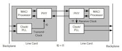
To start, an oscillator is the simplest clock-generation source option. An oscillator only generates a single output frequency for a single component, serving essentially as a single, independent clock. They’re best used for more simplistic systems that only need one or two clocking references. This timing architecture is often utilized for asynchronous applications (Fig. 1).
This type of asynchronous design is ideal for burst-mode traffic applications where fast data transmission is ideal, such as video-processing equipment or campus Ethernet switches. In such an architecture, the oscillators need to have close but not identical frequencies for system operation. If a designer wanted to use an oscillator for continuous communication on the other hand, that would require FIFO management or packet stuffing to avoid issues with data overflow/underflow.
For applications that need faster data speeds, the transmission is much more sensitive to clock jitter, meaning the “jitter budget” shrinks accordingly. Electronical noise from the motherboard and power supply also needs to be considered, as those can impact clock jitter and transceiver performance. To address this, some board designers opt to use a low-dropout (LDO) regulator to provide a clean power source for the oscillator, but this does increase the cost and complexity of the design.
Ultimately, the selection criteria should be based on the acceptable jitter, the desired frequency, and the stability requirements of the application. Particularly for jitter, it’s important to select a clocking reference that provides sufficient margin versus both the typical and maximum reference clock jitter. Conveniently, FPGAs and SoCs usually specify their reference clock requirements in their datasheets, which should be referenced to help drive the selection process.
Generally, though, most applications are going to require multiple timing references, which entails selecting a clock system rather than just an oscillator. Systems
Clock Devices
Integrated clock devices offer numerous advantages over crystal oscillators that make them useful for a range of applications. The component design can be simplified, which speeds up the designing process and reduces costs, and they’re more reliable due to reducing several potential points of failure down to only a single device.
Furthermore, the output frequencies and phase of each output clock can be adjusted, allowing for frequency margining testing and lining up output edges to compensate for signal mismatch. While rarely required features, they do improve the optimization of the timing functionality.
However, this doesn’t mean that integrated clock devices are objectively a better timing solution. A singular clock device that performs all timing still needs its signals to be routed and distributed to other components, requiring the same best practices for optimizing signal integrity as oscillators. These solutions may require extensive analog design expertise, and are quite sensitive to board-level noise, meaning that they must be carefully planned during the design and PCB layout stages.
Despite all of that, for applications that require continuous communication, like cellular infrastructure, data-center switches, and optical networking, an integrated clock solution is usually the best timing option.
There are numerous technologies where it’s ideal for the source and destination to operate at the same frequency. Known as synchronous clocking, it’s often utilized for wired and wireless infrastructure technologies, such as video applications with multiple cameras and video sources that need to be properly coordinated and synchronized within a television studio for broadcast purposes. For these types of synchronous applications, the centralized timing source should provide both primary and secondary reference clocks.
Synchronization to the source ensures that timing is kept consistent and precise across all nodes in the network. Then, phase-locked looping (PLL) is leveraged to lock to the reference clock, remove unwanted electronic noise, and minimize jitter in the clock signal to the downstream device. An example of this functionality can be seen in Figure 2.
This approach not only removes the need for a LDO regulator, but it also provides assurance that the device will provide low-jitter clock synthesis even in the presence of board-level noise. This type of solution is particularly convenient for FPGA-based designs that rely on switched-mode power supplies. Numerous applications, from industrial automation and industrial cameras to test/measurement, medical imaging, defense, and avionics, tend to leverage this approach to timing.
Making a Timing Choice
Many selection criteria and decisions should be considered when evaluating the timing solutions for future designs. In addition to the basic synchronous timing needs of the application, it’s also important to review the environmental noise and potential jitter.
Some clock solutions are more susceptible to environmental noise and require a spread-spectrum clocking design, which reduces electromagnetic interference. Others suffer from highly variable fractional clock jitter that make them unsuitable for in performance-sensitive applications.
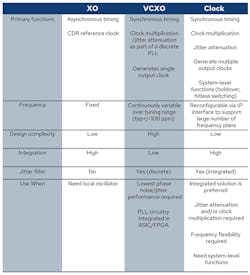
The table below summarizes the selection and provides some high-level guidance on the most suitable timing solution that could meet those needs.


