Alternating Control and Optimizing Bandwidth in Buck-Boost Circuits
What you'll learn:
H-bridge buck-boost ICs are widely used in applications requiring a constant voltage or current source even when the system battery drops to lower voltages. They make sense when a single-stage converter is desired, and the output can be set above or below the input voltage. They can also be used as current sources for LED applications to simplify the design of typical boost-to-buck conversion into a single stage.
These ICs are often favored over other buck-boost topologies, such as single-ended primary inductor converters (SEPIC), due to the cost of the coupled inductor.
True to its name, the H-bridge buck-boost architecture consists of both a buck circuit and boost circuit, united into a single converter. The circuit requires four switches to operate. These four switches are used to regulate the output by sensing the ratio between the output and input to determine the mode of operation.
The H-bridge buck-boost works by operating in one of several modes. When the input voltage is much higher than the output voltage, the circuit will shift into pure buck mode by toggling switches 1 and 2 (Fig. 1). When the input voltage is much lower than the output, the circuit will operate in pure boost mode by toggling switches 3 and 4.
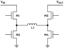
The lines between these modes blur when the input and output voltages are closer together. When the input voltage is close to the output, the circuit will operate in buck-boost mode. In this mode, the four switches can be controlled in several ways to achieve proper regulation.
The Different Operating Modes of Buck-Boost Converters
To determine the operating mode, the circuit senses the difference between the output and input voltage before comparing the ratio to internally set values. Depending on where things stand, the buck-boost converter shifts to different regions. Typically, some hysteresis is given to these values to ensure smooth transitions between different regions due to rising and falling input voltages.
- Buck region: The circuit will operate as a pure buck converter when the internal comparator for this mode triggers due to the output being sufficiently lower than the input. To operate in the buck region, switch 3 must always be closed, and switch 4 must always be open. The first and second switches can then toggle LX1 as they would in a normal forced pulse-width-modulation (FPWM) buck converter (Fig. 2).
- Boost region: The circuit will operate as a pure boost converter when the opposite occurs. The internal comparator for the boost mode triggers when it senses the output is sufficiently higher than the input. To operate in the boost region, switch 1 must remain closed, while switch 2 must always be open. The third and fourth switches can then toggle LX2 as they would in a normal FPWM boost converter (Fig. 3).
- Buck-boost region: When the output is relatively close to the input (either slightly higher or lower), then the circuit will operate in the buck-boost region.
Using Alternating Buck-Boost Control to Tightly Regulate Outputs
With alternating buck-boost control, the circuit will regulate the output by alternating between the buck and boost sides. This means that initially, the circuit will operate the buck switches, and the duty cycle will be set by the comp voltage. The buck switches will operate for a full switching period before the circuit changes to the boost side. Once the buck side has finished a full period, the boost side will toggle with its duty cycle also being controlled by the voltage on comp.
>>Download the PDF of this article, and check out the TechXchange for similar articles and videos

With this operation, both sides of the H-bridge can adjust each buck and boost pulse as needed to regulate the output. It also means that the operating frequency is effectively halved due to each half of the H-bridge toggling only after the other side has finished (Fig. 4).
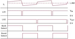
This control method comes with several benefits. The first is efficiency: Because the switching frequency is halved in the buck-boost region, switching losses are minimized. Electromagnetic interference (EMI) is also reduced. Even though the switching frequency is halved, it’s always consistent, which simplifies EMI filtering.
Finally, this approach allows for an improved transient response. That’s because the effective boost duty cycle is lower when the output is slightly higher than the input. Thus, the right half plane zero (RHPZ) in this control scheme is kept at higher frequencies in the buck-boost region.
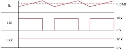
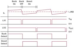
To see how the circuit regulates its output in the buck-boost region, consider the case where the input is slightly higher than the output. The buck-boost cycle starts by controlling the buck side by closing switches 1 and 3. This will cause the inductor current to rise to its peak value with a slope of (VIN – VOUT)/L1.
Once the buck on-time has finished, the control loop will open switch 1 and close switch 2. During the off time of the buck cycle, the inductor current will slew down to its valley value with a slope of VOUT/L1, defining the inductor peak-to-peak ripple.
Once a full switching period elapses on the buck side, the logic circuit will switch over to the boost side. The boost side will start by opening switch 2 and keeping switches 1 and 3 closed. This action represents the off time for the boost. The inductor current during this time will rise in the same manner as the buck on-time with a current slope of (VIN – VOUT)/L1.
Once the boost off-time is finished, the control loop will program the boost on-time by opening switch 3 and closing switch 4. It will cause the inductor current to build back up to the beginning level of the buck on-time with a slope of VIN/L1 (Fig. 5).
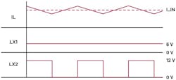
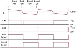
Next, consider the case where VIN is slightly lower than VOUT. Here, each switching period remains the same. The main difference between these cases is that when VIN > VOUT, the inductor current ripple is set by the buck off-time. However, when VIN < VOUT, the inductor current ripple is set by the boost on-time.
The inductor current ripple will also double in the buck-boost region because the frequency of the buck and boost sides of the H-bridge is halved. This is illustrated in Figure 6, as the inductor current completes a full period only after one full buck and boost period have been completed.
The Benefits of the Buck-Boost: Higher Efficiency, Faster Transient Response
In the buck-boost circuit, the overall power-stage efficiency will drop when the circuit enters the buck-boost region. Alternating control can improve the efficiency of the buck-boost region. This happens due to the effective frequency drop during the buck-boost region.
Let’s play it out with an example. During buck operation, if operating at 2.1 MHz, the first and second switches (1 and 2) will both turn on and off once every 476 ns. When operating in the boost region, the same is true for the second pair of switches (3 and 4). When operating in the buck-boost region, nothing changes — except for the fact that the switches are alternating between each side. As a result, the number of switching events stays the same even in the buck-boost region, which boosts efficiency.
To understand how this approach improves transient response of the power supply, look at the scenario in which the output is slightly greater than the input. In this case, the circuit is in the buck-boost region. Since the circuit now boosts more than it bucks, the boost RHPZ will begin to have a greater effect on the circuit. This effect is less pronounced when using alternating buck-boost control, since the inductor current can ramp for a longer time in the boost region.
It also means that changes in the input voltage have less effect on the output because the inductor current can ramp for a longer period to correct for changes in the input more rapidly.
The Trick to Transients: Optimizing the Transient Response of the Buck-Boost
When compensating a buck-boost IC, the selection of the crossover frequency must account for the worst-case load, input voltage, output capacitor value, and inductor value.
Since the buck-boost IC can operate in the boost region, this means that the worst-case VIN will also likely cause the circuit to operate in pure boost mode. When operating in pure boost mode, the circuit encounters an additional limitation in the form of the RHPZ.
The RHPZ is a function of the time delay between charging the inductor and delivering energy to the output; therefore, the loop must be compensated to account for 1/3 to 1/5 of this frequency. Consequently, the transient response of the buck-boost circuit becomes limited, even when more bandwidth is available in the buck region where no RHPZ is present.
Typically, a resistor-capacitor (RC) network consisting of Rcomp1 and Ccomp is used to compensate the control loop and provide the proper phase and gain. To optimize the transient in both boost and buck regions, an extra resistor (Rcomp2) is added to the RC compensation network. A switch is also placed across Rcomp2 to bring it in and out of the compensation network depending on the region of operation.
When the circuit operates in boost mode, the switch will short across Rcomp2, lowering the crossover frequency. When the circuit enters the buck-boost or buck regions, the switch opens, and Rcomp2 helps further increase the gain and phase.
In turn, this will increase the crossover frequency. The operation allows the circuit to have a sufficiently low crossover for the boost region, while also having a sufficiently high crossover for the buck region (Fig. 7).

Designing the Control Loop for a Buck-Boost Conversion Circuit
The control loop for the buck-boost circuit can implemented in multiple ways. One of the most effective is average current-mode control, which provides several benefits that aren’t possible with other control methods.
Noise Immunity
In average current-mode control, the inductor current is sensed and compared against the compensation level. It’s then fed into an inner loop error amplifier that contains an RC compensation network. This integrator provides high gain for the inner loop. The compensated inner loop is subsequently compared against a sawtooth to generate the duty cycle. It leads to higher noise immunity, as any spikes in current in the inductor waveform get filtered out. That’s because the loop is regulating the average current.
Consider the case for peak or valley current-mode control where the sensed inductor current is small relative to the peak or valley value. It results in lower noise immunity since any current spikes present on the sensed current may cause incorrect sampling without some leading-edge blanking or filtering of the sensed current. Even with filtering in place, at low load currents, the slope compensation may become large relative to the sensed signal causing larger deviation in regulation.
Minimum On- and Off-Times
Average current-mode control uses an integrator for the inner current loop with a sawtooth fed to a comparator to generate the duty cycle. Thus, the minimum on- and off-times (TON and TOFF) can be much smaller compared to peak current mode or valley current mode, which will have larger min on- and off-times due to having circuits such as leading-edge blanking.
No Slope Compensation
Importantly, the average current-mode control approach doesn’t require slope compensation. This simplifies the maximum current limit, since it’s no longer a function of the added slope. Because no slope compensation is needed, this also means that average current mode has better performance in discontinuous conduction mode (DCM) when compared to peak current mode, where the slope compensation can become a large part of the sensed signal.
Parallel Operation
If multiple converters are intended to run in parallel, then average current-mode control provides the best current sharing. That’s because the outer loop will program the average current of each converter, whereas peak or valley current mode will have some offset in the current in each converter due to their slightly different inductances.
Put to the Test: Evaluating a Buck-Boost Converter Design
Let’s look at an example design. The goal is to create a buck-boost converter that accepts an input voltage (VIN) from 6 to 18 V and delivers a regulated 13-V output at 2.5 A, while keeping the output capacitance as low as possible. The target peak-to-peak ripple in the output voltage is ±5%.
To minimize the output capacitance, start by selecting a switching frequency of 2.1 MHz. At this speed, 1 µH is typically used for the inductor value. The VOUT limits allow for a 650-mV transient. To estimate the output capacitance required, first start by considering the worst-case VIN, which will put the circuit in the boost region. In the boost region, the RHPZ can be calculated using Equation 1.

By calculating the RHPZ and dividing the total by 5, the crossover frequency in the boost region will be set at 35 kHz. Equation 2 can be used to estimate the output cap. By solving this equation, the output cap is estimated at 17.5 µF. Round this value up to 22 µF. With the components selected, the comp can now be designed starting in the boost region to achieve a 35-kHz crossover.

Once Rcomp and Ccomp are selected, the circuit must be compensated for the buck region at 18 VIN. Since there’s no RHPZ, select the crossover frequency to be 100 kHz. Rcomp2 can then be adjusted to achieve this crossover.
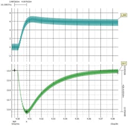
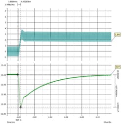
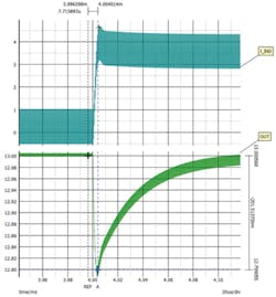
With everything in place, the transient response in each case is checked. The transient in the buck and buck-boost regions is reduced due to the addition of Rcomp2. This is depicted in Figures 8, 9, and 10.
Conclusion
Alternating buck-boost control has the edge over standard control methods due to its improved transient response, higher efficiency, and reduced EMI, as well as its design simplicity. The transient response of the buck-boost circuit can be further optimized with the addition of Rcomp2 to help improve loop bandwidth.
>>Download the PDF of this article, and check out the TechXchange for similar articles and videos
About the Author
Mark Derhake
Applications Engineer, Analog Devices
Mark Derhake is an applications engineer with over three years of industry experience. He graduated from Southern Illinois University, Edwardsville, with his bachelor’s degree in electrical and computer engineering in 2020. In 2021, he joined Maxim Integrated (now part of Analog Devices) to work on LED products, including matrix managers, LED current sources, linear LED regulators, and integrated buck-boost ICs.
Comment About the Article
To join the conversation, and become an exclusive member of Electronic Design, create an account today!

Leaders relevant to this article: