EDA Helps Cultivate the Future of Die-to-Die Connectivity

Check out our coverage of DesignCon 2024. This article is also part of the TechXchange: Chiplets - Electronic Design Automation Insights.
Today, many of the world’s most advanced processors are no longer single monolithic slabs of silicon. They’re comprised of a collection of smaller silicon die commonly referred to as chiplets that use advanced 2.5D or 3D packaging to mimic a single large chip.
On the edge of every chiplet is a PHY that enables high-bandwidth, low-latency connectivity with the other devices in the package, which all interact with each other over proprietary or industry-standard protocols. As success in the semiconductor industry becomes more about what companies can cram into a package instead of a monolithic chip, the quality of these die-to-die (D2D) interconnects, typically based on high-speed SerDes, can make or break the design.
While they typically bridge very short distances, these D2D interconnects send data around the package at high speeds. This can negatively impact the bit error rate (BER) in the channel as well as the performance of the chiplets.
Keysight Technologies is trying to stay a step ahead with a new simulation tool called Chiplet PHY Designer, which I learned about first-hand at DesignCon 2024. Using it, Keysight said chip designers can quickly and accurately validate the PHY-based D2D interconnects in a package before investing in actual silicon from a foundry.
The ability to model and test D2D connectivity is key to the future of heterogeneous chip design. Doing so helps make sure the chiplets inside a 2.5D and 3D package can interact seamlessly.
“Chiplet PHY Designer accelerates validation of chiplet subsystems, from one D2D PHY through interconnect channels to another D2D PHY, much earlier in the design cycle,” said Niels Faché, VP and GM of Keysight EDA.
Chiplet PHY Designer is the latest tool in Keysight’s Pathwave ADS platform for high-speed digital design and simulation. It’s also uniquely able to verify that chiplets meet the Universal Chiplet Interconnect Express (UCIe) standard. UCIe is one of several emerging standards in D2D interconnects. UCIe gives the chiplets an easier way to communicate, reducing friction when it comes to mixing and matching IP from third parties.

The company said Chiplet PHY Designer presents a faster and easier way to simulate the electrical performance of D2D interconnects based on UCIe and test out designs against the latest revisions of the specification.
What are the Pros and Cons of Chiplets?
Flexibility is a hallmark of chiplet technology, said Stephen Slater, product manager for Keysight’s high-speed digital simulation technology. The concept of chiplets allows companies to adapt to evolving markets and new technological advancements by mixing and matching chiplets, he told Electronic Design.
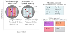
Instead of placing everything on a single slab of silicon as usual, the movers and shakers in the semiconductor industry are breaking up complex systems-on-chips (SoCs) into smaller silicon dies that have separate pieces of IP, including CPUs, GPUs, AI accelerators, memory, I/O, and various other chip functionalities. After being tested, verified, and validated, the chiplets can be mixed and matched in a package using silicon interposers or other 2.5D packaging technologies, such as TSMC’s CoWoS or Intel’s EMIB, or more advanced 3D stacking.
In many cases, companies are pulling apart these larger processors and repackaging them because they’re too expensive or impossible to build on a single silicon die due to the physical limits of Moore’s Law. By spreading out the SoC’s functionality over several chiplets, you can cram more transistors in the package than you can in a single processor due to the “reticle limit” of the wafer manufacturing process, said Slater.
The chiplets themselves interact with each other using high-speed, short-range SerDes PHYs and establish connections over UCIe or various other die-to-die interfaces such as the Open Compute Project’s (OCP) Bunch-of-Wires (BoW) and the Common Electrical I/O (CEI) Extra-Short Reach (XSR) standard.
Dismantling SoC designs into a smaller set of chiplets makes for easier heterogeneous integration, noted Slater. Every chiplet can be built on the best process technologies for the job, helping reduce complexity and costs.
As process technology continues to evolve, specific chiplets can be upgraded while others are left alone. Slater added that the capacity of chiplets for swift customization and upgrades means faster time-to-market and lower costs.
He said chiplets are also physically smaller than the large SoCs that they are stripped out of. Consequently, a larger number can be manufactured per wafer without imperfections, increasing yields. Higher yields translate to lower production costs.
Partitioning a processor design and repackaging the building blocks in a way that mimics a monolithic chip is no easy feat. These chips resemble SoCs on a module, and so they tend to be vulnerable to signal integrity, timing, and other issues that are more often encountered by system integrators. Dissipating heat from these IC packages is also complicated, requiring thermal simulation both early in the design and during integration into products.
But the pros tend to outnumber the cons for advanced heterogeneous chip designs. Chiplets are considered key to the future of high-performance chips required for everything from artificial intelligence and machine learning (AI/ML) to augmented reality (AR).
UCIe: Bridging the Connectivity Gap for Chiplets
Chiplets are unlocking a new wave of innovation in chips. The issue for the semiconductor industry is the lack of a standard plug-and-play way for chiplets to communicate once they’re bound together in an IC package.
Today, companies tend to use proprietary D2D interconnects and protocols that lock them into using IP designed internally or sourced externally and then validated and tested in-house. In short, they lose the flexibility they’re accustomed to with third-party IP. While they still have the freedom to use any foundry’s packaging technologies, using third-party chiplets can be more trouble than it’s worth without a standard D2D interface.
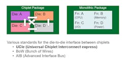
UCIe presents one way to solve these problems. It fills the gap for industry-standard D2D interconnect that allows for the mixing and matching of chiplets—no matter the company that designed it, the foundry that manufactured it, or the type of advanced packaging (2D, 2.5D, or 3D) used. First released in 2022, the UCIe spec covers the physical I/O with data paths on physical bumps grouped into lanes to the protocol stack as well as everything required for testing and validating the D2D interconnect.
The goal is to create a vibrant ecosystem for chiplets, so that companies can buy and sell each other’s pre-validated chiplets and plug them into a package almost as seamlessly as components on a circuit board. Instead of spending money on a full SoC, engineers can focus on developing the specific chiplets they need and rely on commoditized technologies for other aspects of their chip designs. Call it the “chiplet economy.”
UCIe is already being supported or adopted by many of the top semiconductor equipment and electronic design automation (EDA) vendors as well as leading foundries and chip designers like AMD, Intel, NVIDIA, and TSMC.
The Role of Keysight’s EDA Software in Chiplet Design
With Chiplet PHY Designer, Keysight is catering to semiconductor companies with a stake in UCIe’s future.
The test-and-measurement giant said it adapted its high-speed digital design and simulation technology to help deal with the single-ended signaling and forwarded clocking of UCIe-based D2D interconnects.
Chiplet PHY Designer can automatically parse the signals traveling through the UCIe-based interconnect. It’s also able to automate wiring connections between the chiplets inside the package to evaluate and perhaps improve the signal integrity. Furthermore, according to Keysight, the EDA software supports a standard-driven simulation setup such as speed grade and a special probe component for more intuitive measurement setup.
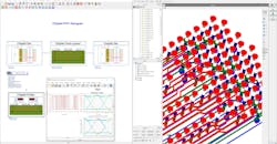
Chiplet PHY Designer can also model and simulate the voltage transfer function (VTF) of the interconnect—a ratio of the input voltage of a signal as it enters the interconnect to output voltage on the other side—to make sure that the PHY meets the UCIe standard. Since it’s influenced by signal loss and crosstalk, the VTF must be measured very accurately to guarantee the delivery of signals from one PHY to another, said Slater.
Keysight said Chiplet PHY Designer helps companies accurately model and simulate D2D interconnects, and it’s accurate enough to rival the precise time-domain measurements of high-speed oscilloscopes—it can assess the BER of the system to within 1e-27 or 1e-32. It can also measure eye diagram height, eye width, skew, mask margin, and BER contour. The term “eye diagram” refers to the pattern of a high-speed signal.
By meeting the latest IBIS modeling specification for electrical I/O, physical integrators can dig even deeper into the PHY electrical validation process, leveraging detailed models to do “pre-silicon” performance predictions.
Check out more of our coverage of DesignCon 2024 and more articles in the TechXchange: Chiplets - Electronic Design Automation Insights.
About the Author

James Morra
Senior Editor
James Morra is the senior editor for Electronic Design, covering the semiconductor industry and new technology trends, with a focus on power electronics and power management. He also reports on the business behind electrical engineering, including the electronics supply chain. He joined Electronic Design in 2015 and is based in Chicago, Illinois.
Comment About the Article
To join the conversation, and become an exclusive member of Electronic Design, create an account today!

Leaders relevant to this article: