Empower the Next Wave of Semiconductor Reuse Through Chiplet Realization
What you'll learn:
- Discover how chiplets are transforming semiconductor design by opening the door to reusable, scalable, and cost-effective solutions.
- Learn about the growing importance of standardization, advances in EDA tools, and the role of chiplets in physical AI systems.
- Explore the challenges and opportunities shaping the future chiplet marketplace.

Chiplets are clearly on the minds of system-on-chip (SoC) and electronic systems designers. Case in point: Cadence’s eBook titled “Cadence Chiplet Solutions — Helping You Realize Your Chiplet Ambitions” was downloaded more than 500 times in its first month.
Chiplets enable a marketplace of reusable semiconductor die, allowing system designers to aggregate complex functions through package-level scaling. The resulting chips deliver immense functionality with unprecedented time-to-market, at a fraction of the typical cost for a monolithic chip design.
They’re predicted to enable massive semiconductor reuse, assuming a large-scale chiplet marketplace is realized. The question isn’t whether such a marketplace will materialize, but when it will materialize and what it will take for that to happen.
To understand the future of chiplets, it’s worth pausing and touching on the user profile for multi-die designs and chiplets. Multi-die design is an established semiconductor design technique spearheaded by the data center, cloud infrastructure, and AI/high-performance computing (HPC) markets.
In this model, users typically design all die in the system, managing everything from design and manufacture to packaging. They sometimes utilize proprietary die-to-die interfaces or customize them to specific needs, treating die reuse as a nice-to-have, rather than a must-have.
On the other hand, chiplet users are unlikely to design all dies in the system. Instead, they’re looking to outsource some or all of them, relying on standardization across die-to-die interfaces and packaging to ensure interoperability. These chiplet aggregators are likely planning multiple product SKUs from the same set of die and expecting future die reuse across numerous product generations.
Many applications utilize multi-die technology, with mature usage seen across data centers, cloud, and AI. The use of chiplet-based architectures across these applications continues to expand, primarily for I/O disaggregation, with several off-the-shelf chiplet solutions available for designers. As the importance and complexity of I/O and memory interface designs ramps up, designers seek ways to accelerate design schedules without the need to build deep in-house expertise.
Enter Physical AI
Physical AI — the combination of automotive, robotics, drones, and aerospace and defense — looks to be the next big adopter of chiplets, which provide an effective path to enable scalable edge AI-capable devices. Acquiring a silicon-proven chiplet die for these essential functions and package integrating, rather than designing from the ground up, achieves these goals.
>>Check out this TechXchange for similarly themed articles and videos
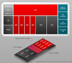
With physical AI system silicon, the main system functions neatly disaggregate into logical partitions such as CPU processing, AI engines, and system utilities (I/O, memory). These die building blocks make possible a flexible chiplet system architecture covering a multitude of designs, including autonomous systems, object detection, natural language processing (NLP) and interpretation, and physical action applications (Fig. 1).
With the value proposition apparent, what’s holding back widescale marketplace evolution and chiplet availability? Several factors play into this, including the fear of being first, standardization convergence, and a bit of a technology gap, all of which are solvable in my opinion.
Some companies don’t have the time or money to risk adopting a relatively unproven chiplet system solution. Instead, they’re waiting for silicon proof. In addition, these companies don’t want to fund such a development themselves, preferring to let someone else assume the development cost and prove the system. Only then will they adopt a similar architecture that matches their needs.
Comprehensive Specifications Accelerate Adoption
With the introduction of more comprehensive and inclusive specifications, much progress on chiplet system architecture standardization has been made in the past few years. However, many items are still to be determined. Competing specifications remain, too, and adoption hasn’t yet driven convergence on a single standard over another.
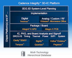
Huge technology innovations have emerged over the years, including the availability of EDA tools that more seamlessly handle the increased complexities of chiplet-based design and verification (Fig. 2). Packaging technologies also continue to grow in capabilities and maturity, yet interoperability between package types remains a challenge.
Looking ahead, expect the challenge gaps to close significantly, but not fully. (Hey, we have to be realistic — this is a journey, not a milestone.) Companies that fund reference platforms will pave the way for lower-risk adoption of chiplet-based architectures. Chiplet system architecture specifications that promote open and CPU-neutral interfaces will accelerate the convergence of standardization, setting the stage for individual chiplet providers to build interoperable solutions that feed into a chiplet marketplace.
Combined with a focus on building reference platforms, this will lead to innovative chiplet architecture frameworks that simplify standards-based chiplet design. Continued EDA and IP advances will reduce the complexity adoption barrier for chiplet-based designs by providing increased automation and repeatable flows.
The industry is on the verge of realizing the full potential of chiplets, which is to enable the aggregation of complex functions through package-level scaling. Looking ahead, we can expect to see the industry continue streamlining chiplet-based design and unlocking its immense potential. As for when that chiplet marketplace will emerge and facilitate large-scale adoption, time will tell, but the essential groundwork will be laid in 2026.
>>Check out this TechXchange for similarly themed articles and videos
About the Author

Mick Posner
Senior Product Marketing Group Director, Chiplet and IP Solutions, Cadence Design Systems
Michael "Mick" Posner brings three decades of deep expertise to his role as Senior Product Group Director in Cadence's Compute Solutions Group, where he spearheads innovative chiplet and IP solutions that are reshaping the semiconductor landscape.
With his comprehensive background spanning digital front-end to mixed-signal back-end design, Mick has witnessed and driven the evolution of electronic design automation from its early days to today's cutting-edge multi-die architectures. His specialized focus on chiplet technologies positions him at the forefront of industry innovation, helping engineers tackle the most complex design challenges.
A graduate of the University of Brighton in England with a B.S. in Electronic and Computer Engineering, Mick combines technical excellence with practical industry experience. His unique perspective, developed over 30 years in the EDA and IP space, makes him an invaluable voice in discussions about the future of semiconductor design and the technologies that will power tomorrow's most advanced systems.
Comment About the Article
To join the conversation, and become an exclusive member of Electronic Design, create an account today!

Leaders relevant to this article: