Accelerating Semiconductor/Electronic Systems with Comprehensive AI Digital Twins
What you'll learn:
- Current challenges facing the semiconductor industry.
- The transition to software-defined designs for semiconductors and electronic systems.
- Why using a comprehensive digital twin is the best way to achieve success.
Siemens EDA is a major provider in the electronic design automation (EDA) space. They provide solutions ranging from hardware-assisted verification to analog testing to hypervisors. With the dynamic growth and ubiquity of electronic systems globally, software-defined, AI-powered, and silicon-enabled technologies are critical for today’s semiconductor industry, which is projected to reach $2 trillion by 2035 according to industry analysts.
I talked with Craig Johnson, Vice President of Strategy at Siemens EDA, about the challenges facing the semiconductor industry and how AI-powered comprehensive digital twins can help with the design of silicon-enabled systems.
What’s happening in today’s EDA industry with regards to the semiconductor industry and the CHIPS and Science Act, to help vitalize the U.S. semiconductor industry with innovation and economic advances?
Modern technological products cannot exist without semiconductors. As crucial and essential components that power systems and devices in our electronically connected world, semiconductors are essential to technologies such as artificial intelligence, electric vehicles, clean energy, aerospace, and defense.
Increasing demand for smaller, faster, and higher-performance chips, plus AI integration to develop smarter products faster, are pushing the boundaries of electronic design and manufacturing capabilities, including cost efficiency and sustainability goals. Today, the semiconductor industry is facing the complexities of design requirements, limited resources, sustainability regulations, and supply-chain issues, adding to design cycle constraints and challenges.
Our customers are trying to figure out how to compress their designs into more predictability, from 18 to 36 months to 12 to 18 months for development and delivery. So we’re striving to reduce time-to-market chip and semiconductor development with AI-powered software solutions.
The industry is transitioning toward software-defined products and systems, such as the automotive sector, where software can provide differentiation to meet consumer preferences. How does a software-defined approach apply to the semiconductor industry?
The big trend across industries is the transition to software-defined design for electronic systems and semiconductors. Systems integrators are seeking value by product differentiation through software — for example, in the automotive industry with autonomous driving, infotainment features, driver assistance, voice commands, safety functions, and personalized driver and passenger experiences.
Automotive OEMs now need to determine how to design and simulate these capabilities for optimum performance under these complex systems of systems, using software for product personalization and differentiation starting with semiconductors. The traditional approach of designing hardware first and then adapting the software to it is no longer feasible with the advancements in modern computing, AI, and other high-performance applications.
Software-defined systems are transforming the landscape of electronics development with hardware now dependent on software architecture. Software workloads drive hardware architecture decisions from the earliest stages of design, where virtual representations of the semiconductor require experimentation to understand the compute platform that best optimizes the software.
Adopting a software-defined methodology enables engineering teams to configure the entire system with software, including scaling limitations, multi-domain design and optimization, and maintaining data links across different levels of IC and system integration. This is an exciting opportunity for companies leveraging EDA software as a competitive advantage over established companies that must adapt to a faster pace while dealing with legacy operations.
Digital transformation and shift-left engineering are essential in the competitive global economy. To effectively manage design complexity and deliver advanced electronics systems, companies must adopt strategies that encompass production-grade AI, efficient requirements capture and modeling, and methodologies that support software/hardware co-design.
As chip-level scaling faces constraints, the integration of chiplets and 3D IC design workflows is crucial. We’re seeing a major shift in the semiconductor industry and addressing these challenges with robust software-defined, AI-powered, silicon-enabled solutions.
How is Siemens EDA enabling AI-powered multi-domain design engineering?
Developing next-generation semiconductors is an expensive process, but necessary because more electronic systems and products rely heavily on software. As the world’s demands for semiconductor-enabled products and systems ramp up, the complexity of designing, manufacturing, and implementing ICs, advanced IC packaging, and printed-circuit-board (PCB)-based systems are increasing exponentially.
Companies need to embrace a multi-domain engineering approach. This involves integrating software, mechanical and electronic design to manage the growing complexities of system-of-systems development.
AI is integral to closing this semiconductor engineering gap by connecting systems capabilities for operations, networking, power management, security, monitoring, learning, verification, validation, and testing across domains. Managing cross-domain data within the context of a silicon lifecycle necessitates integration with broader platforms, while also gaining domain-specific insights.
For example, design engineering planning for the scalability and flexibility in software and electronics platforms are essential for product lifecycle management. With software-defined engineering, teams can monitor and impact real-world operating conditions as the product is in full operation. Integrating active monitors in semiconductors allows manufacturers to track performance and reliability, ensuring that products operate as intended and maintain up-to-date functionally throughout their product lifecycle.
For decades, we have been deploying AI, at-scale, for computer chip design and manufacturing to help our customers deliver better products globally and provide an array of AI-powered software tools.
How does a digital twin apply for semiconductor design and manufacturing?
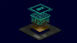
The foundation of successful digital transformation is the implementation of the comprehensive digital twin. It’s a physics-based digital representation of a process or a product — a virtual copy of a physical or soon-to-be physical thing.
Siemens is the industry leader for enabling the comprehensive digital twin that encompasses all cross-domain models and data, from mechanical CAD and CAE to software code, bills of materials, bills of process, and more. This holistic approach creates a precise virtual representation matching the physical form, functions, and behavior of products and their configurations.
Customers who adopt a comprehensive digital-twin approach significantly reduce the need for physical prototypes during development by defining and optimizing the product and production systems, saving valuable time and resources. Updates to the digital twin reflect any changes to its physical counterpart throughout the product lifecycle, establishing a closed feedback loop between the virtual and real environment. This provides the continuous optimization of products, production, and supply-chain processes cost-effectively.
With such seamless integration of products and production, including software and automation, manufacturers can design, simulate, test, and validate products using a comprehensive digital twin to optimize product and process quality while reducing design cycles. Semiconductor and systems companies can achieve more than just visual fidelity or simulation accuracy — it’s the unprecedented breadth and depth of integration across domains, processes, and lifecycles.
Where many EDA software vendors offer fragmented capabilities limited to specific functions or processes, a comprehensive digital twin delivers a connected ecosystem spanning design through operation.
Siemens’ comprehensive digital-twin enablement delivers a virtual representation of the product or process flow that matches the exact physical form, functions, and behavior of the product and its configurations, while participating across the product and process lifecycle to simulate, predict, and optimize the product and production system. Most critically, it connects real-world operational data back into product design and production over the lifetime of the product, creating a self-improving system that most digital software vendors cannot provide.
Additionally, software-defined digital threads enable numerous processes across multiple systems, providing a connected dataflow across the lifecycle of a product from design to manufacturing and beyond.
Digital threads consolidate isolated data into collective intelligence for the comprehensive digital twin. By mirroring the physical world in the virtual world with digital threads, engineering teams can predict the performance and optimize the product in a proven and secure manner. Thus, automation of tasks is achieved, and functions are interconnected, integrated, and linked so that engineering teams can quickly access, share, and manage their program details across the entire product lifecycle.
These digital threads provide a complete end-to-end process for a given industry, such as electronic systems and the semiconductor ecosystem. With the comprehensive digital twin and digital threads, companies will have a real-time digital backbone for design optimization, verification implementation, manufactured deployment, and maintenance of these complex systems of systems.
Siemens is unique in providing both best-in-class PLM and EDA software, hardware, and industry expertise and services that address specific complexity needs of our electronic systems and semiconductor customers and their partners.
What additional software technologies is Siemens EDA exploring for the semiconductor market?
As electronics and semiconductor manufacturers navigate increasingly complex market demands, supply-chain disruptions, and sustainability imperatives, the comprehensiveness of digital-twin implementations is a critical differentiator, preparing a company to quickly integrate emerging technologies into processes.
Leveraging data from throughout the organization makes data streams accessible to key decision-makers. It provides greater transparency and the perfect ecosystem to integrate industrial AI and industrial metaverse applications.
Industrial AI can automate mundane tasks, accelerate product and process evaluation, and help users learn new tools. This is particularly crucial with the aging and retiring workforce, engineering talent shortages, and skill gaps. And anticipated for the future of manufacturing, the industrial metaverse would combine digital twins, AI, and software-defined automation to create an intuitive and collaborative virtual design-and-build environment.
Major pressures across industries are anticipated to continue, and recent geopolitical tariffs are likely to impact global business, particularly for the electronics and semiconductor sectors. As manufacturers face increasing costs, design complexities, global sustainability mandates, and engineering resource constraints, digitalization and new technologies are required to keep pace with innovation and time-to-market goals.
Companies that invest in a holistic digital transformation mindset throughout their organizations will realize powerful and sustainable advantages with digital twins that integrate processes into transparent and unified business operations. The comprehensive approach provided by Siemens EDA is a strong and reliable foundation for future industrial and technological transformation.
About the Author

William G. Wong
Senior Content Director - Electronic Design and Microwaves & RF
I am Editor of Electronic Design focusing on embedded, software, and systems. As Senior Content Director, I also manage Microwaves & RF and I work with a great team of editors to provide engineers, programmers, developers and technical managers with interesting and useful articles and videos on a regular basis. Check out our free newsletters to see the latest content.
You can send press releases for new products for possible coverage on the website. I am also interested in receiving contributed articles for publishing on our website. Use our template and send to me along with a signed release form.
Check out my blog, AltEmbedded on Electronic Design, as well as his latest articles on this site that are listed below.
You can visit my social media via these links:
- AltEmbedded on Electronic Design
- Bill Wong on Facebook
- @AltEmbedded on Twitter
- Bill Wong on LinkedIn
I earned a Bachelor of Electrical Engineering at the Georgia Institute of Technology and a Masters in Computer Science from Rutgers University. I still do a bit of programming using everything from C and C++ to Rust and Ada/SPARK. I do a bit of PHP programming for Drupal websites. I have posted a few Drupal modules.
I still get a hand on software and electronic hardware. Some of this can be found on our Kit Close-Up video series. You can also see me on many of our TechXchange Talk videos. I am interested in a range of projects from robotics to artificial intelligence.

Craig Johnson
VP, EDA Strategy, Siemens EDA
Craig Johnson joined Siemens in 2021 and is the VP of Strategy for Siemens EDA. He joined Cadence in 2004where he held leadership roles in strategic planning, marketing, M&A, and IT. Prior to Cadence, Craig worked in strategic marketing and operations at Intel. Craig holds MBA and B.S. degrees in electrical and computer engineering from Brigham Young University.
Comment About the Article
To join the conversation, and become an exclusive member of Electronic Design, create an account today!

Leaders relevant to this article: