The Missing Handoff Between Schematic Generation and PCB Layout Automation
What you’ll learn:
- Why the deeper opportunity for AI in hardware design is workflow redesign, not simply faster drawing or routing.
- How a shared system model allows topology, component, circuit, and documentation agents to work in parallel.
- Why an enriched netlist can carry enough engineering intent to improve the handoff from schematic generation to PCB layout.
Artificial intelligence is making its way into a lot of engineering workflow, yet hardware development has responded more slowly than software. Even when AI appears in an electronic-design workflow, it’s often treated as a smarter component-search tool, an automatic router, or an assistant that explains how a circuit works.
Those functions are useful, but they don’t represent the more important change. The deeper opportunity is not to ask AI to imitate an engineer drawing one schematic page at a time. It’s to reorganize hardware development from a serial chain of specialists and documents into a requirements-driven system where several focused agents can work in parallel.
The handoff between schematic generation and PCB layout is a useful place to see why that change matters. It exposes the difference between logical design and physical implementation, but it also exposes a wider coordination problem: Important decisions are created throughout the workflow, while the information needed to act on them is often passed downstream only after another stage has been completed.
The Distance Between a Schematic and PCB
A schematic and a PCB describe the same product from different dimensions. The schematic records components and their electrical connections. It describes the functional intention of a circuit — which device provides power, which pins communicate, and how the circuit is divided into functional blocks.
The PCB is the physical expression of that intention. It must account for the actual shape and size of components, where they’re placed, and how copper connects them on a real board. A connection that looks like a simple line on a schematic may become a routing, current-carrying, thermal, or placement problem in the physical design.
In many teams, the electronics engineer designs the schematic and a layout engineer designs the PCB. The schematic and netlist are intended to serve as the bridge between them. Ideally, the schematic also communicates which signals are critical, whether certain nets need length matching or impedance control, how much current a power path carries, and how sensitive signals should be treated.
In practice, much of that information is communicated in meetings, messages, or live reviews rather than recorded in a reusable form. The conversation isn’t simple information transfer. It requires the team to translate abstract logical intent into physical instructions, and that translation depends heavily on the experience shared by the engineers involved.
Why the Traditional Workflow Stays Serial
A conventional workflow usually follows a familiar order: requirements, architecture, component selection, schematic capture, netlist export, PCB placement and routing, simulation, and iteration. Different specialists may own different stages, but each person normally waits for an upstream artifact to become stable enough to use.
This organization creates three recurring problems:
- Serial dependency: The layout engineer is expected to wait for the schematic to be sufficiently complete before beginning serious work, even when some system boundaries and placement questions could have been explored earlier.
- Experience as a black box: Component selection and circuit decisions often depend on an engineer’s memory of availability, pricing, packages, reliability, and prior designs. This knowledge is valuable but difficult to reproduce or share consistently.
- Repeated translation: If a package, thermal condition, or signal-integrity issue is discovered during layout, the question returns to the schematic owner. A decision that could have been made at the architecture stage is instead discovered late and travels backward through the process.
The problem is therefore larger than whether the schematic and PCB tools can exchange a netlist. The workflow itself delays useful information and forces engineers to repeatedly explain context that could have been captured earlier.
A requirements-driven workflow contrasts with that serial flow. It doesn’t eliminate reviews or engineering judgment. It changes when work can begin and gives each participant a shared model of the system before starting detailed implementation.
A Requirements-Driven Multi-Agent Workflow
In a parallel workflow, the starting point is a set of natural-language or formal requirements that can be converted into a system-level model. The model identifies functional blocks, interfaces, voltage domains, power budgets, timing assumptions, and the important decisions or risks that still need human review.
The resulting block diagram is no longer only a presentation graphic. It becomes a working agreement among the agents and engineers. Once an engineer approves the system boundaries, several roles can proceed at the same time:
- A topology agent defines the major functional blocks and their connection relationships.
- A component-selection agent evaluates candidate parts against electrical requirements, package constraints, availability, price, and lifecycle information.
- Circuit agents design individual modules, perform calculations, and check the local design assumptions.
- A drawing and documentation agent converts reviewed electrical connections into a consistent schematic and keeps the shared artifacts synchronized.
The agents don’t work independently without limits. Their work is coordinated through the approved system model. An interface between two modules must have the same voltage, protocol, and timing assumptions on both sides. A part choice that changes the power budget or package must be visible to the other modules it affects.
A prompt-to-KiCad workflow such as the one developed at SpeedUp is one implementation of this idea. The important result is not that a prompt produces a drawing — rather, requirements, architecture, component choices, calculations, schematic pages, and downstream design information should remain connected and reviewable.
The Smart Netlist as a Shared Deliverable
A traditional netlist primarily records logical connectivity. It tells the design system that one pin is connected to another. In the workflow proposed here, the final schematic and netlist package can carry additional engineering information, becoming what this article calls a “smart netlist.”
The term doesn’t require a new universal file format. It describes an enriched, structured handoff whose data remains linked to the relevant components, nets, and functional modules. Depending on the design, it may include:
- Routing priority and signal type, including differential pairs and sensitive signals.
- Specific length-matching or other handling requirements.
- Current levels for power paths and the resulting routing implications.
- Functional grouping and placement suggestions for modules or sensitive components.
- Assumptions that must be confirmed before the physical design is released.
When a PCB tool or PCB-design agent receives this package, it doesn’t begin from connectivity alone. It receives part of the reasoning that produced the connectivity. This is the missing handoff between schematic generation and layout automation — not a finished PCB and not an instruction to remove the layout engineer, but a more complete starting point for physical design and review.
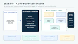
Example 1: A Low-Power Sensor Node
Consider a request to design a low-power temperature-and-humidity sensor node with a microcontroller, sensor, battery, power conversion, and debug interface. The first output should not be a page of placed schematic symbols. The system first needs a topology, module definitions, power rails, a power budget, important signals, and a list of decisions, assumptions, and risks.
After the engineer reviews the block diagram, the agents responsible for the individual modules can work in parallel. The power agent is able to evaluate the battery and regulator. The sensor and microcontroller agents define their circuits and interface. The component agent can compare packages, availability, and cost. The drawing agent will assemble the approved modules into a consistent schematic.
As the figure shows, the resulting handoff to PCB design includes more than the MCU-to-sensor connections. It can identify the current class of the battery and regulated rails, the nature of important signals, the grouping of the functional modules, and any sensitive or heat-producing parts that should not be placed together. The layout engineer or PCB agent still decides how to realize the board, but less intent is left to informal explanation.
Example 2: A Wireless Controller
The same method applies to a small wireless controller containing a microcontroller, USB interface, power conversion, memory, and an antenna. The system model defines the major modules and interfaces first. Module agents can then evaluate and design their portions concurrently instead of waiting for a single engineer to finish the entire schematic.
The enriched handoff will identify the USB interface as a critical signal group, keep the power-conversion module distinct from the wireless section, and preserve the intended relationship among the antenna, controller, and board boundary. These aren’t attempts to complete the layout inside the schematic. They’re examples of information that should survive the transition from logical design to physical design.
The Engineer Becomes the Technical Director
This workflow doesn’t reduce the importance of the engineer. It changes where engineering attention is most valuable. Instead of spending most of the process manually carrying information from one document or specialist to another, the engineer defines the architecture, approves system boundaries, checks calculations, reviews component choices, and resolves conflicts among the agents’ outputs.
The traditional engineer is comparable to a person laying every section of railway by hand. In a multi-agent workflow, the engineer plans the network and directs several construction teams working from the same map. The work proceeds in parallel, but the engineer remains responsible for the map, the interfaces, and the final technical decisions.
Seen this way, the missing handoff between schematic generation and PCB layout is one part of a broader workflow redesign. The netlist evolves from a list of connections into a carrier of shared engineering intent. Once that intent is explicit and reviewable, AI can do more than draw faster: It helps hardware teams coordinate work that previously had to proceed one stage at a time.
About the Author
Ruiwen Dong
Electronics Engineer, SpeedUp
Ruiwen Dong is an electronics engineer at SpeedUp, where she works on AI-assisted circuit-design workflows that turn product requirements into structured, editable KiCad schematic projects. Her work focuses on schematic generation, design handoff, component and interface constraints, and the engineering review required before PCB layout.
Comment About the Article
To join the conversation, and become an exclusive member of Electronic Design, create an account today!
 Leaders Logo
Leaders relevant to this article: