The eGaN® FET-Silicon Power Shoot-Out Vol. 7: Buck Converters

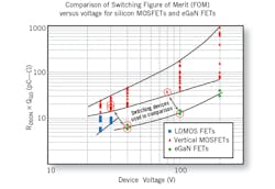
fig. 1
we can see that eGaN FETs have a significant advantage over the MOSFETs across the entire voltage range. However, when considering switching FOM alone, the advantage at 200 V seems to diminish compared to state-of-the-art MOSFETs. The actual in-circuit performance advantage of eGaN power devices, however, could be even larger due to its lack of diode reverse recovery (QRR) [4]. In contrast, at the lower end of the eGaN FET voltage range, the in-circuit performance advantage may actually be less dramatic than the FOM suggests due to the reduced importance of QRR and the increased importance of the body diode forward voltage drop.
Furthermore, as the required device voltage decreases below that of the currently available eGaN FET voltage range, other silicon switching solutions such as LDMOS-based devices (with or without vertical termination) become a viable alternative, but eGaN FET technology is still in an early stage of development and as it progresses it will lead to greater and greater performance advantage at both lower and higher voltages. In this article, two different voltage conversion range buck applications are presented and their results compared with similar state of the art silicon MOSFET devices.
Low-voltage buck application
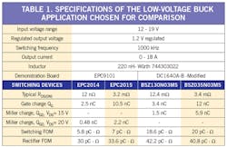
There are many point-of-load (POL) applications suited for buck converters that typically operate from either 5 V or 12 V supply rails. At lower voltage and current, the power MOSFETs can be monolithically integrated, while hybrid modules and discrete solutions are popular for higher currents and voltages. Depending on the required load power, currents of up to 20 A per phase are typical, although single phase outputs as high as 40 A are possible. For higher load currents, such as voltage regulation modules (VRM), multiple buck phases are interleaved to improve efficiency and dynamic response. Faster dynamic response and the higher bandwidths demanded by the evolving power architecture of V-core and other sensitive loads will influence the faster adoption of eGaN FET-based POL solutions. The megahertz range of switching frequencies achievable enables the use of smaller inductors and capacitors, thereby offering smaller size and lower systems costs for eGaN FET-based POL Systems. Portable applications running off batteries (10 V – 12 V) specify a minimum efficiency requirement that must be complied with, yet compatibility with an external adapter typically requires 19 V operation; all this while operating within thermal design limits. This 19 V input requirement means that 30 V (or higher) MOSFET devices are required. Although load voltages vary, it is customary to compare converters at 1.2 V output.
For this comparison, an EPC9101 eGaN FET demonstration board [5] was used and compared to the same buck controller’s MOSFET demonstration board DC1640A-B [6], which was modified to match the EPC9101’s input and output capacitors, inductor and operating frequency. Furthermore, the default MOSFETs were also replaced with MOSFETs of similar RDS(ON) as the eGaN FETs. Photos of these boards as tested are shown side-by-side in Fig. 2.

fig. 2
Input and output voltage was measured as close as possible to the actual converter circuit using the voltage sensing terminals provided on the boards. A summary of the test setup is given in Table 1.
Since the higher forward voltage of eGaN FETs body diode is of concern in this application, when first measuring efficiency the dead-time was increased to include approximately 10 ns of body diode conduction at each switching edge (20 ns per cycle). A 3 A Schottky diode was also added in parallel with the EPC2015 device and the efficiency was measured again. The 12 V and 19 V input efficiency results for these test conditions are given in Fig. 3 and Fig. 4, respectively.
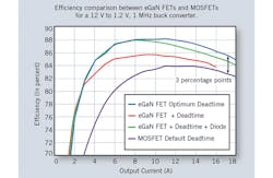
fig. 3
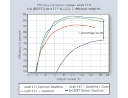
fig. 4
The addition of roughly 20 ns of diode conduction per cycle decreased the eGaN FET based converter efficiency by about two to three percentage points over the input voltage range. At light load (below 3A) however, the efficiency actually increased slightly as this additional dead-time allowed for self commutation of the switch-node voltage. Using a small amount of dead-time for optimum full load operation also meant that forced commutation occurred at light load [7]. The addition of a Schottky diode significantly improved efficiency and was almost as effective as optimizing the switch timing. Under all tested operating conditions the eGaN FET-based converter’s efficiency was higher than that of the equivalent MOSFET circuit by between three and seven percentage points. In fact, optimum eGaN FET operation at 19 V input yielded higher efficiency than the equivalent MOSFETs operating at 12 V input.
Mid-voltage Buck application
For higher voltages beyond the capability of 30 V MOSFETs, the application space becomes varied with no specific high-volume applications. Almost all telecom converters use -48 V supplies, thus requiring isolation for step-down to +12 V or +24 V bussing; while for computing and networking equipment that use a positive 48 V bus, the use of a buck converter is possible only where there are no mandatory isolation requirements. Regardless of the actual application, the MOSFET and eGaN FET can still be compared for this mid-voltage range by considering a more generic buck application given in Table 2.

For comparison, two mid-voltage Buck demonstration boards [8, 9] were used to compare the eGaN FETs with MOSFETs. Both standard demonstration circuits were modified to have identical input and output capacitors, inductor and operating frequency. A photo of the two boards side-by-side as tested is shown in Fig. 5.
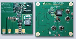
fig. 5
As with the low-voltage comparison, the MOSFET devices were also replaced with MOSFETs of similar RDS(ON). For accuracy, the input and output voltages were measured as close as possible to the actual converter using added terminals. Table 2 summarizes the test setup for the mid-voltage Buck demonstration boards.
The efficiency and equivalent power loss results are shown in Fig. 6 and Fig. 7, respectively.
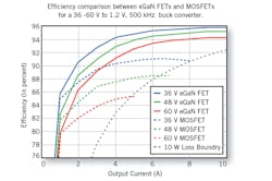
fig 6.

fig. 7
Measurements were taken with up to 10 A of output current, or until total converter power loss reached 10 W; whichever occurred first. These results clearly show the significant improvement of between four and eight percentage points in efficiency between MOSFETS and eGaN FETs. More telling is the fact that at the points where the MOSFET-based converter power losses reach 10 W, the eGaN FET-based converter losses are less than half by comparison — reducing power converter loss by 50%.
Both low-voltage and mid-voltages converters showed a significant improvement in efficiency of between three and eight percentage points, although this improvement is more dramatic for the mid-voltage comparison. These results clearly show that this generation of eGaN FETs offers a distinct advantage over vertical MOSFET devices for device voltages down to 30 V.
References
- Johan Strydom, Andrew Ferencz, “eGaN® FET-Silicon Power Shootout Vol. 3: Power over Ethernet”, Power Electronics Technology, March 2011
- Johan Strydom, Andrew Ferencz, “eGaN® FET-Silicon Power Shoot-Out Vol. 4: Brick Converters”, Power Electronics Technology, July 2011
- Johan Strydom, Andrew Ferencz, “eGaN® FET-Silicon Power Shoot-Out Volume 6: PoE-PSE Converter”, Power Electronics Technology, Nov. 2011
- Johan Strydom, Andrew Ferencz, “eGaN® FET-Silicon Power Shoot-Out Part 1: Comparing Figure of Merit (FOM)”, Sept. 2010, Power Electronics Technology, July 2011
- Efficient Power Conversion EPC9101 demonstration circuit
- Linear Technology DC1640A-B demo board
- Johan Strydom, Bob White, “High Step-Down Ratio Buck Converters With eGaN Devices”, How2Power Today, Nov 2010
- National LM5116 demonstration circuit from Texas Instruments
- National LM5113 demonstration circuit from Texas Instruments
Related Articles
eGaN® FET- Silicon Power Shoot-Out Volume 6: PoE-PSE Converter
GaN Powers MOSFET Figure of Merit Past Silicon-Based Devices
eGaN(tm)-Silicon Power Shoot-Out: Part 1 Comparing Figure of Merit (FOM)
About the Author
Strydom
Johan
Comment About the Article
To join the conversation, and become an exclusive member of Electronic Design, create an account today!

Leaders relevant to this article: