Characterizing Performance Of Mid-Voltage GaN-on-Si Devices
Recently, much attention has been paid to the commercial advent of 600 V rated GaN-on-Si based power devices [1,2]. This is, in part, due to the many obvious advantages of such devices over their silicon and silicon carbide based alternatives. Principally, the large advantage in performance/cost such as $/mΩ of on-resistance of nearly a factor of 10 compared to Si superjunction or SiC FETs.
Related Articles
- 600 V GaN on Si-Based Power Use GaNpowIR®
- Commercial 600V GaN-Based Power Devices Coming of Age
- Cascode Configured GaN Switch Enables Faster Switching Frequencies And Lower Losses
There has been, however, much less discussion of the significant benefits of GaN-on-Si based power devices at substantially lower voltage ratings, for instance between 80 and 250 V. One reason for this may be the relatively small and highly segmented market for these medium voltage devices, some $1 billion, compared to the nearly $5 billion market for 600 V rated power devices. In addition, the advantage of medium voltage GaN based power devices may not be as apparent as at higher voltages, where the higher breakdown field strength of the materials involved in the GaN based HEMTs provide a clear advantage in on-resistance when compared to silicon based alternatives.
At device ratings of 80 to 250 V, the main performance advantage of GaN based HEMTs over silicon FETs is the nearly 100-fold improvement in minority carrier reverse recovery charge (Qrr). In fact, there are negligible holes present in the operation of GaN based HEMTs. While, this is also true for SiC based FETs, the very low channel mobility and expensive cost structure of these devices makes SiC FETs non-viable for wide spread commercial adoption at voltages below 1200 V.
LINEAR SWITCHING
The near complete absence of minority carriers in the operation of GaN based HEMTs using high mobility two dimensional electron gas transport between source and drain ohmic contacts results in essentially purely capacitive, highly linear switching behavior of the devices. This, in turn, eliminates the ringing induced in circuit and allows for very high speed, nearly square wave, switching. It should be noted that the normally off 100 V devices currently being sold by International Rectifier are a cascoded combination of a 100 V rated GaN HEMT and a low voltage silicon MOSFET. As such, there is a minority carrier contribution to Qrr from the silicon FET built in body diode. This Qrr is about 3 nC and is some 100 times less than that of the best in class 100 V rated uni-polar silicon MOSFETs.
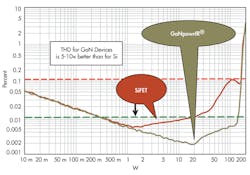
As has previously been shown [3], 100 V rated cascoded GaN based devices switch cleanly within about 1 to 2 ns for a 70 V transition. Such nearly ideal switching characteristics are highly prized in several power conversion applications. One such application is the class –D audio amplifier circuit, where the lack of fidelity to clean square wave switching degrades the audio output signal. Such lack of fidelity is measured as total harmonic distortion (THD). A comparison between the THD measured for 100 V rated best in class silicon based FETs and first generation GaNpowIR® cascoded HEMTs are shown in Fig. 1. As can be seen, a 5 to 10 fold reduction in THD is achieved using the GaN based devices. Such dramatic improvement in audio output quality has driven rapid adoption of GaN based devices into commercial class-D audio systems [4].
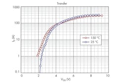
Due to the lateral nature of the GaN based HEMTs, there has been some concern over the ability of the device layout to scale to higher current handling capability or to very low on-resistance. To address these concerns, an initial effort was made at International Rectifier to demonstrate large, high current device fabrication and performance. Fig. 2 shows the measured transfer characteristics of a nominally 10 mΩ, 100 V rated cascoded GaN HEMT. Such devices exhibit saturation currents of more than 300 A at room temperature.
In fact, saturation currents of approximately 450 A has been measured for these devices with applied gate bias to the silicon cascode FET of +10 V.
Lower On Resistance, Gate Charge
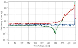
For 250 V rated devices, the advantages of GaN based devices over silicon alternatives such as unipolar MOSFETs or superjunction FETs is a combination of substantially lower specific on-resistance, lower output charge (Qoss), dramatically reduced and highly linear reverse recovery charge (Qrr) as well as reduced gate charge (Qg). Such devices are well suited as primary as well as secondary side switches in some AC:DC conversion circuits. The breakdown voltage characteristics of such a 250 V rated cascoded GaN based HEMT power devices with a gate width of 877 mm and a nominal on-resistance of 13 mΩ is shown in Fig. 3.
As can be seen, the drain to source leakage current is well below 1 nA/ mm of gate width, even to a drain to source voltage of nearly 400 V, where some evidence of punch-through behavior may be evident. The gate leakage current is very well behaved to less than 1 nA/mm until evidence of dielectric breakdown, which determines the reliable operating limits of the device, can be seen occurring near 500 V drain bias.
As no JEDEC certified standards for GaN based power device reliability qualification currently exist, it is imperative that the behavior of such devices be tested under long term stress for periods far in excess of the standards used for well established silicon based technology platforms. It is well known that the 1000 hour tests commonly applied to silicon devices at 80 % of rated voltage and 150 °C is based on an established failure activation energy of about 0.8 eV. As such, the accelerated stress relates to some 10 years of operation at an average temperature of 85 °C.
There is no data to suggest that the activation energy of GaN based devices is also about 0.8 eV. Therefore, no claims of long term reliability of GaN based devices can legitimately be made at this time based on successful application of the silicon based standard.
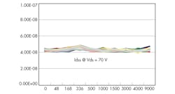
As reported in 2010[5], over 10,000,000 device-hours with up to 10,000 hours of standard long term stress testing per device were successfully achieved for low voltage (20 to 30 V) rated GaN HEMTs. Similar results have been obtained for medium voltage rated devices. Fig. 4 shows the stability of the drain leakage current for 100 V rated cascoded devices for stress conditions of 80 V drain bias at 150 °C for up to 9000 hours. To date, over 5,000,000 device hours of biased reliability testing have been achieved for the 100 V technology node.
It should be noted that 600 V rated GaN based devices have also successfully achieved more than 5000 hours of long term stress testing [2]. These data represent a substantial basis for establishing the intrinsic reliability of GaN based power HEMTs.
The inherent differences in the nature of GaN based HEMT and high performance silicon based vertical FETs, lead to unavoidable and revolutionary advantages of the GaN based alternative. The low magnitude and high linearity of terminal capacitances, together with the essential absence of minority carriers in the GaN based HEMTs provide for clean, fast switching which eliminate the need for filters or transition rate limiting gate resistors, providing far superior characteristics compared to the incumbent silicon based devices.
References
[1] M.A. Briere, Power Electronics Technology, July 2011 pp 26-28
[2] M.A. Briere, Bodo’s Power Systems, May 2013 pp 48-50
[3] M.A. Briere, Power Systems Design, April 2012 pp.20-24
[4] International Rectifier Commences Commercial Shipments of Gallium Nitride on Silicon Device, International Rectifier Press Release May 9, 2013 http://www.irf.com/whats-new/nr130509.html
[5] M.A. Briere, Bodo’s Power Systems, Nov 2010 pp. 22-25
