eGaN® FET – Silicon Power Shoot Out: A Retrospective
In mid-2010, GaN FET technology was made available to the general power conversion engineering community when Efficient Power Conversion (EPC) introduced the industry’s first commercially available GaN power transistor. Since that time, EPC has continued on two parallel paths – one to expand their portfolio of products and the other to share what it learns about the use of the technology with power conversion systems design engineers. One of these educational efforts has been to work with the editors of Power Electronicsmagazine and publish a bi-monthly series of articles on the characteristics of GaN technology and its applications.
This series is entitled eGaN FET -- Power Silicon Shoot Out. Articles in the series took on both basic issues and specific applications using gallium nitride components. It is timely to make a quick review of the fourteen articles to make certain that we have accomplished the goal of assisting engineers in climbing the learning curve. This retrospective look will give us insight into what further topics and studies are needed to advance the adoption of GaN technology, the need to learn is never finished.
Related Articles
- Where are the High Voltage GaN Products?
- GaN Transistors :Thermal Management, Drive Control and Isolation Techniques
- Characterizing High Power Semiconductors Requires New Technologies
- Quality, Robustness and Reliability of 600 V GaN-on-Si Power Devices
GaN BASICS
The articles started with an introduction to the basics of GaN technology, with discussions on Figures of Merit (FOM) allowing the comparison of GaN transistors with industry-standard silicon-based MOSFET technology. An issue that accompanies any new technology is the need to understand the idiosyncrasies of the new technology. For example, in the case of gallium nitride, how to drive the high frequency GaN FET, methods for optimizing dead time, determining the effects of board layouts on overall power conversion performance and the impact parasitics play in degrading efficiency.
The initial article, “Figures of Merit (FOM),” appearing in September 2010, defines several measurements that can be used to compare power devices. MOSFET manufacturers have used FOMs for years to show both generational improvements and competitive devices. FOMs are helpful because no matter what the die size, the FOM is almost constant for a given technology or device generation.
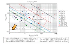
In addition, this article discussed the basic electrical, thermal and mechanical characteristics of gallium nitride power devices. These new devices were compared with state of- the-art silicon and an example of the comparisons, the Switching FOM, is given in Fig. 1. The eGaN FETs offered a significant reduction in FOM compared to aging silicon (Si) power devices.
eGaN FETs enable much higher switching speeds than their silicon counterparts, thus the different requirements for gate drive, layout, and thermal management had to be explored. The second article, “Drivers, Layouts” took on this subject. The article points out that, when considering gate drive requirements, the three most important parameters for eGaN FETs are the maximum allowable gate voltage, the gate threshold voltage and the body diode voltage drop.
The article concludes that the maximum allowable gate-source voltage of 6 V is low compared with traditional silicon. The gate threshold is also low compared to most power MOSFETs, but does not suffer from as strong a negative temperature coefficient. Third, the “body diode” forward drop can be a volt higher than comparable silicon MOSFETs, requiring a smaller dead time than MOSFET based designs.
Further, the article examined the gate drive requirements, layout, and thermal design considerations important to designers wanting to develop products that leverage the superior attributes of gallium nitride transistors.
“Optimizing FET On-Resistance” provided a means for quickly and efficiently determining optimal eGaN FET on-resistance and enabling the designer to select a suitable eGaN FET by comparing available devices to an optimum value. Within the article, a die size optimization process is discussed and an example application is used to show specific results. Optimum has different meanings to different people, so the process presented aimed at maximizing switching device efficiency at a given load condition.
Using the simple optimization method presented is a quick way to find the optimum eGaN FET on-resistance value. Since eGaN FETs will always optimize to a lower on-resistance than MOSFETs, the overall peak efficiency will therefore be higher (i.e. total conduction and switching losses equal at peak) than MOSFETs with the given assumptions. If the same on-resistance is used, the eGaN FET efficiency will peak at a lower current.
Another article, “Optimizing Dead Time” looks at the impact that dead time has on system efficiency for both eGaN FETs and MOSFETs. Gallium nitride devices perform significantly better by most metrics, although the eGaN FET body-diode forward voltage is higher than its MOSFET counterparts. This can be a source of significant loss in high current, high frequency applications. The article explains that body diode forward conduction losses alone do not make up all dead-time dependent losses, but that diode reverse recovery and output capacitance losses are also important. The article went into depth on dead-time management and the need to minimize all dead-time losses.
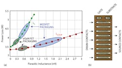
Due to the high switching speed of gallium nitride transistors, the impact of parasitics, package inductances and high frequency loop inductance of the PCB layout become critical factors to consider in reducing overall losses. In a two-article series entitled “Impact of Parasitics” and “Optimal PCB layout,” these critical factors were explored. Specifically, the first article studied the effect of parasitic inductance on the performance of eGaN FETs and MOSFETs in point-of-load buck converters switching at 1 MHz. Taken from the first article, Fig. 2 showed the impact of parasitic inductance on performance and how the chip-scale (LGA) package used for the eGaN FET lowers the power loss.
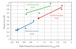
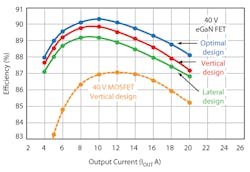
The second article, “Optimal PCB layout,” examined various PCB layout designs to control the high frequency loop inductance. Different layouts with similar common source inductance and different high frequency loop inductances are compared and methods to reduce loop inductance by PCB layout were proposed. The article documented a real-life example that showed that optimizing PCB layout for an eGaN FET-based point of load (POL) buck converter with reduced parasitics lead to improved efficiency, faster switching speeds, and reduced device voltage overshoot compared to conventional MOSFET based designs. Figs. 3 and 4 show the reduction in high frequency loop inductance and the increase in efficiencies that were achieved from various layout designs.
Paralleling transistors is a technique power converter designers use to increase system performance. Because gallium nitride FETs can be switched ten times faster than commercial MOSFETs, paralleling GaN FETs pose a host of new challenges. In an article dedicated to “paralleling,” the problems and recommendations for achieving optimum results were presented.
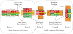
The first installment, “Paralleling eGaN FETs--Part 1,” of a two-part article covering the subject, presented five basic designs utilizing four EPC2001 (100 V, 25 A) paralleled devices per switch in a half-bridge configuration. These layouts are given in Fig. 5. The merits and drawbacks of each in terms of parametric factors are discussed. A finding of this article is that the fundamental question of whether high frequency GaN FETs can be connected in parallel is shown to be “yes.”
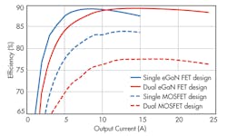
In the second installment, “Paralleling eGaN FETs--Part 2,” a 1 MHz buck converter was demonstrated using paralleled eGaN FETs and compared with state-of-the-art silicon devices in a similar circuit. To evaluate the performance difference between paralleled MOSFETs and eGaN FETs, a synchronous buck converter with an input voltage up to 19 VDC and an output of 1.2 V was built and tested. The efficiency results are shown in Fig. 6.
Applying the lessons learned in the first installment, the second part showed that connecting two eGaN FETs in parallel can yield converter performance on par with single device equivalents and provide results far better than can be achieved with state-of-the-art silicon MOSFETs.
APPLICATIONS
The eGaN FET – Power Silicon Shoot Outseries of articles went beyond examining the basic principles of the technology and complemented theoretical discussions with analyses of design challenges and measured performance results for eight power conversion application topics. Sharing experimental setup and test result comparisons with MOSFETs, these application-focused articles provided a chance to examine GaN FETs in practical circuits. The applications ranged from ubiquitous buck converters to a state-of-the-art wireless power transfer system.
It is commonly held that, as the voltage requirement of an application increases, the performance advantage of using eGaN FETs also increases. The article, “Buck Converters,” demonstrates that, when comparing the switching Figure of Merit (RDS(ON) x QGD) between silicon FETs and eGaN FETs versus voltage, the eGaN FETs have a significant advantage over MOSFETs across the entire voltage range as shown in Fig. 7 from the article.
Isolated brick converters are widely used in telecommunication systems to provide operating power to network equipment. These bricks come in a variety of standard sizes and input and output voltage ranges. Most can operate over large input voltage ranges of 2:1 or even as high as 4:1. Their modularity, power density, reliability and versatility has simplified and to some extent commoditized the isolated power supply market.
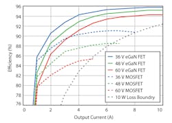
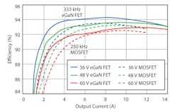
In volume 4 of the Shoot-out series, “Isolated DC-DC Brick Converters,” a prototype eGaN FET-based fully regulated eighth brick converter was compared to a similar MOSFET-based converter. The eGaN FET demonstrated improved efficiency and 15% more output power at a 33% higher switching frequency as shown in Fig. 8.
In addition to the advantages provided by eGaN FETs in hard switching isolated and non-isolated applications, an article dedicated to “High Frequency Resonant Converters” shows the ability of the eGaN FET to improve efficiency and output power density in soft switching applications. The article compares results using eGaN FETs to what is achievable with existing power MOSFET devices.
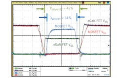
The device output charge has a direct impact on the energy required to achieve zero voltage switching (ZVS). A reduction in energy required to achieve ZVS can result in reduced dead time, shown in Fig. 9, providing a larger power delivery period and lower RMS currents in a high frequency resonant converter. Due to a factor of almost two decrease in output charge provided by eGaN FETs, the ZVS transition is achieved in a proportionally shorter period, increasing the effective duty cycle and improving the overall converter performance.
The third article in the series, “Power over Ethernet,” demonstrates that eGaN FETs are a viable and efficient alternative to standard MOSFET solutions in Power over Ethernet (PoE) applications. Gallium nitride transistors enable higher operating frequencies that can be leveraged into reduced converter size and cost. For this article, both 13 W and 26 W PoE eGaN FET converters were built and evaluated side by side with standard MOSFET designs. In every instance, eGaN FET converters exhibited higher efficiencies with the potential of reducing system cost over their MOSFET counterparts.
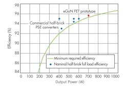
One article in the series, “Power-over-Ethernet Power Sourcing Equipment” (PoE-PSE) was dedicated to examining this demanding isolated converter application with higher device voltage requirements. Operating at about twice the device switching frequency, an eGaN FET-based, fully regulated, half-brick PSE converter prototype outperformed a comparable state-of-the-art MOSFET-based commercial converter. The eGaN-based converter had an output power 100 watts more than the closest MOSFET-based commercial converter shown in Fig. 10.
In this PoE-PSE converter article, the isolated brick converters were considered with a particular focus on eighth-brick converters where size constraints are most severe. These isolated brick converters are widely used in telecommunication systems to provide operating power to network equipment and are available in various standard sizes, input and output voltage ranges. What they all have in common is that the input and output power devices are all rated at 100 V or lower. These converters benefit even more from the advantages that eGaN FETs brings with increasing voltage rating.
Beyond the traditional silicon MOSFET power converter applications where it was shown that gallium nitride transistors have the potential to improve the efficiency of DC-DC conversion, a new technology needs to provide increased performance that enable applications that were not possible (or were extremely difficult) with existing technology. Gallium nitride technology achieves this requirement and the Shoot Out series introduced several new applications enabled with its high frequency switching capability. Two such applications are envelope tracking, which significantly improves efficiency of RF power amplifiers and wireless power transfer, where high switching frequency is needed to meet the industry’s operating standards exceeding 6 MHz.
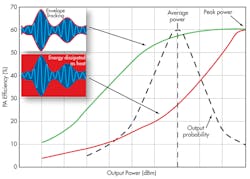
Envelope tracking for radio frequency amplifiers is not new. But with the ever increasing need for improved cell phone battery life, better base station energy efficiency, and more output power from very costly RF transmitters, the need for improving the RF power amplifier system efficiency has become an intense topic of research and development. The key to improving efficiency lies in the amplifier’s peak to average power (PAPR) requirements. As shown in Fig. 11, it is possible to achieve peak efficiencies as high as 65% with a fixed supply, but given PAPRs as high as 10, the average efficiency is likely to be lower than 25%. Through modulation of the amplifier’s supply voltage, this can be improved to over 50% - essentially doubling the efficiency and reducing losses by two thirds! This will not only reduce power consumption, but also lower the cost of operation, cooling requirements, and size.
Another application, wireless power, is gaining popularity in many commodity products such as mobile phones chargers and drive-over electric car charging mats. Recently there has been a push for operation in the restricted and unlicensed lower ISM band at 6.78 MHz and this is where traditional MOSFET technology is approaching its capability limit. In this application, enhancement mode gallium nitride transistors offer an alternative to MOSFETs as they can switch fast enough to be ideal for wireless power applications.
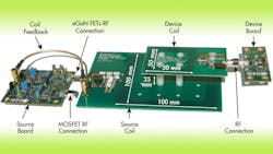
The “Wireless Power Converters” article presented an experimental evaluation of a highly resonant coil wireless energy system using eGaN FETs in a half bridge topology operating at 6.78 MHz, designed to be suitable for multiple 5 W USB based charging loads. In the article, an experimental system, shown in Fig. 12, was compared to a similar unit based on equivalent MOSFETs in the power converter stage. Using eGaN FETs in the power amplifier yielded a 4% amplifier efficiency improvement over the MOSFET version and a 24% reduction of power losses.
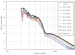
The most recent article examined the “RF Performance” of the 200 V power switching EPC2012 eGaN FET. Unlike power switching FETs, RF FETs are designed to work best in the linear region of operation to maximize power gain and minimize distortion, whereas power-switching devices are optimized for lowest RDS(ON) and gate charge. Another significant difference between power switching and RF FETs is the power dissipation capability of RF devices significantly higher than that of power switching devices for equivalent terminal characteristics to accommodate the higher power losses in the linear region.
The article, which focused on RF characterization in the frequency range from 200 MHz through 2.5 GHz, found that although the eGaN FET is optimized as a power-switching device, it exhibits good RF characteristics (Fig. 13); and future eGaN FET parts can be optimized for better RF performance at higher frequencies.
LOOKING AHEAD
The 14 articles in the Shoot-out series are a good start to assisting engineers up the learning curve of this new and exciting gallium nitride technology. But more work is needed and, with the help of universities reporting their foundational research and companies sharing their hard-earned empirical results, the future for the expansion of GaN education in the engineering community is as promising as the technology itself.
As educational materials on GaN technology become available, EPC will continue to publish articles. Further, EPC is maintaining a GaN library to which all who are interested can contribute and have access through epc-co.com. Gallium nitride technology provides superior performance and has the potential to take power conversion to the next level of performance – we just need to keep climbing the learning curve.
The entire Shoot-out series of articles on GaN FETscan be viewed on the Power Electronics website, at http://powerelectronics.com.
Voice Your Opinion!
To join the conversation, and become an exclusive member of Electronic Design, create an account today!

Leaders relevant to this article:
