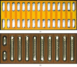
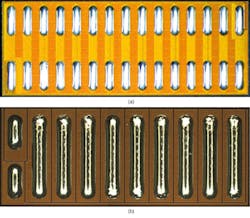
A significant upgrade in performance usually designates semiconductor products as part of a new generation of devices. In most cases this involves semiconductor process improvements and may include packaging refinements. Efficient Power Conversion’s (EPC) new Gen 4 eGaN FETs follows this scenario with its chipscale LGA footprint (Fig. 1a) that improves on its Gen 2 eGaN FETs (Fig. 1b). Interleaved drain and source bars of Gen 4 reduce power loop inductance while internal design virtually eliminates common source inductance. As shown in Fig. 1a, the largest devices of the Gen 4 family include a gap between the top row and bottom row solder bars.
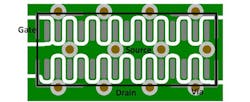
This gap in the middle of the die enables large copper traces along with cooling vias that enhance thermal performance in the associated PCB. Fig. 2 shows a sample layout for a 2 ounce copper top layer. Using 12 mil vias with 22 mil annular rings on 1.6-mm centers helps remove the heat from the area surrounding the device as well as from the center of the transistor. This configuration also supports the use of our optimal layout power loop structure when using 4 ounces or more of copper on the inner layers.
Related Articles
- eGaN FET Development Board Uses Dedicated GaN FET Gate Driver
- eGaN® FET Family Adds 100 V, 16 milliohm Power Transistor
- GaN Transistors – Drive Control, Thermal Management, and Isolation
- Application-focused Gallium Nitride (GaN) Transistors Textbook
- 600-V GaN transistor gets JEDEC stamp
- GaN Transistors Reach the 600V Operation Plateau
Previously, if you wanted to increase the output current capability of a FET-based DC-DC converter, you would have to parallel multiple output power devices. Although paralleling high performance eGaN devices does provide higher output power, it also increases parts count, adding cost and complexity while reducing system power density. The Gen 4 family of eGaN FETs exhibits a significant reduction in on-resistance, (RDS(ON)), which enables high current and high power density from a single eGaN FET. Table 1 compares RDS(ON) as well as other parameters for both generations of devices.
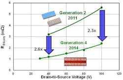
Fig. 3 compares the on-resistance of Gen 2 and Gen 4 eGaN FETs as a function of drain-to-source voltage (VDS). In Fig. 3, the Gen 4 eGaN FETs rated from 40 V to 100 V have an on-resistances ranging from 1.2 to 2.4 mΩ. The Gen 4, 200 V EPC2019, has a typical on-resistance of 33 mΩ in an ultra-small footprint.
Hard Switching
In a traditional hard-switching eGaN FET, switching losses are primarily impacted by:
· QGD, the gate-to-drain charge (also known as the Miller charge), which controls the voltage rising and falling transition time
· QGS2, the portion of the gate-to-source charge from the device threshold voltage to the gate plateau voltage, which controls the current rising and falling transition time.
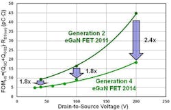
A common yardstick for comparing performance of various FETs is their figure of merit, FOM, based on their product of on-resistance, RDS(ON), and gate charge. From a processing standpoint, RDS(ON) and gate charge are interrelated, if one goes down the other goes up, and vice versa. Therefore, better devices have a lower FOM. The hard switching figure of merit (FOMHS) compares the in-circuit performance capability of a given device technology in a hard-switched application. Here:
FOMHS = (QGD + QGS2) × RDS(ON) (1)
As shown in Fig. 4, the Gen 4 eGaN FETs provides an almost 2x reduction in FOMHS over Gen 2.
When compared to the best state-of-art Si power MOSFETs this Gen 4 family reduces FOM by 3.5x, 6.1x, and 8.5x, respectively for 40 V, 100 V, and 200 V devices. With lower FOMHS, improved device packaging, and low parasitic PCB layout, the high frequency performance of Gen 4 eGaN FET-based converters exhibit a significant improvement over converters employing Si MOSFETs.
In most soft-switching applications, the device output charge, QOSS, impacts performance because it directly affects the energy required to achieve ZVS (zero voltage switching). A reduction in energy required to achieve ZVS can result in reduced dead times and ZVS currents, providing both a larger power delivery period and lower RMS currents in high frequency soft-switching and resonant converters. QOSS is also the main loss component in ZCS (zero current switching). The other major contributor to loss is total gate charge, QG, which is a major switching related loss in high frequency soft-switching applications.
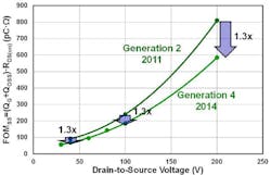
In resonant and soft-switching applications, the switching-related losses are minimized by using techniques such as ZVS and ZCS. With reduced switching losses, the FOMHS used for hard switching applications is no longer valid for soft-switching applications. Therefore, you should compare GaN vs. silicon MOSFET performance with the soft switching figure of merit, FOMSS, which is:
FOMSS = (QG + QOSS) × RDS(ON) (2)
Gen 4 eGaN FETs provide 1.3X reduction in FOMSS over the previous generation, as shown in Fig. 5.
When compared with the best state-of-art Si power MOSFETs, the Gen 4 eGaN FETs reduce FOM by 1.7x, 2.3x, and 3.5x, respectively, for 40 V, 100 V, and 200 V devices. With lower FOMSS, improved device packaging, and low parasitic PCB layout, the high frequency performance of high density eGaN FET-based converters is significantly improved, compared with Si MOSFET-based converters in soft switching as well as hard switching applications.
Miller Ratio
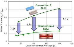
Significantly higher voltage and current slew rates can impact eGaN FET performance. Therefore, these conditions must be well-understood in order to fully utilize the technology. A high, positive-voltage slew rate (dv/dt) on the drain of an off-state device can occur in both hard- and soft-switching applications, and is characterized by a quick charging of the device capacitances. This dv/dt event charges the drain-source capacitance (CDS). Concurrently, it also charges the gate-drain (CGD) and gate-source (CGS) capacitors in series. Unless you address this issue the charging current through the CGD capacitor flows through and charges CGS beyond VTH (gate threshold voltage) and turns the device on. This event, sometimes called Miller turn-on, can be very dissipative.
To determine the dv/dt susceptibility of a power device, you can evaluate a Miller charge ratio (QGD/QGS1) as a function of drain-to-source voltage. A Miller ratio of less than 1 guarantees dv/dt immunity. Fig. 6 shows the large reduction in Miller ratio in Gen 4 FETs, with a value of 1 at half their rated voltage.
Experimental Results
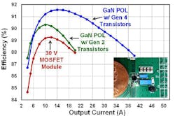
To demonstrate the improved performance of Gen 4 eGaN FETs, two buck converters were constructed using a combination of the Generation 4 eGaN FETs as the synchronous rectifier and Generation 2 eGaN FETs as the control device. The first of these converters combined the 30 V, EPC2023 (Gen 4) with the 40 V EPC2015 (Gen 2) in a 12 V to 1.2 V DC-DC point of load (POL) converter. A second example was an intermediate bus converter (48 V to 12 V) constructed with an 80 V EPC2021 (Gen 4) combined with a 100 V EPC2001 (Gen 2). Table 1 lists their characteristics.
Shown in Fig. 7 are the experimental results of the 12 V to 1.2 V, 40 A POL converter operating at switching frequency of 1 MHz achieving efficiencies above 91.5% provides superior in-circuit performance of the Gen 4 eGaN FETs compared with the Gen 2 eGaN FETs (shown in green), and state-of-the-art Si MOSFET modules (shown in red).
DC-DC Efficiency
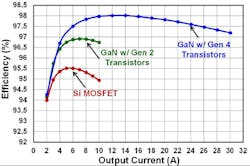
Fig. 8 shows the experimental results of the 48 V to 12 V, 40 A, non-isolated DC-DC intermediate bus converter operating at a switching frequency of 300 kHz. It achieves efficiencies above 98%, again significantly outperforming the Gen 2 eGaN FETs, shown in green (Fig. 8), and state of the art Si power MOSFETs, shown in red. This 48 V to 12 V intermediate bus converter shows great resilience to higher frequencies with an efficiency of 96% at 1 MHz.
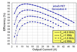
Improved performance also enables higher frequency operation without sacrificing an enormous amount of efficiency. Fig. 9 shows the 12 V to 1.2 V buck converter efficiency at various PWM frequencies. At 0.5 MHz, the converter achieves almost 94% peak efficiency. This peak efficiency drops to 87.5% at 2 MHz.
About the Author

Sam Davis
Sam Davis was the editor-in-chief of Power Electronics Technology magazine and website that is now part of Electronic Design. He has 18 years experience in electronic engineering design and management, six years in public relations and 25 years as a trade press editor. He holds a BSEE from Case-Western Reserve University, and did graduate work at the same school and UCLA. Sam was the editor for PCIM, the predecessor to Power Electronics Technology, from 1984 to 2004. His engineering experience includes circuit and system design for Litton Systems, Bunker-Ramo, Rocketdyne, and Clevite Corporation.. Design tasks included analog circuits, display systems, power supplies, underwater ordnance systems, and test systems. He also served as a program manager for a Litton Systems Navy program.
Sam is the author of Computer Data Displays, a book published by Prentice-Hall in the U.S. and Japan in 1969. He is also a recipient of the Jesse Neal Award for trade press editorial excellence, and has one patent for naval ship construction that simplifies electronic system integration.
You can also check out his Power Electronics blog.
