Enabling Industrial and Automotive Multimegahertz Buck Converters with GaN
Recent trends in buck converters include switching at higher frequencies to improve transient response, reduce magnetic size, and control EMI. High switching frequencies are quite common with 12V buck converters, where silicon transistors are sufficiently advanced to enable efficient multimegahertz converters. But in the 24 to 60V space—comprising industrial, automotive and telecom applications—silicon transistors are not efficient enough to use in multimegahertz buck converters. Instead, gallium nitride (GaN) transistors enable superior efficiency and performance, enabling 2 to 2.5MHz buck converters operating from 48V buses.
Because of GaN’s significantly reduced switching losses (both in terms of reduced output capacitance and reduced switching time), buck converters using GaN can be switched around five times as fast as those using traditional silicon power transistors.1 Additionally, GaN transistors do not suffer from reverse recovery, which creates significant current spikes (generating EMI) and power losses during hard-switching transitions. In this article we examine the benefits of GaN for 48V input buck converters targeting high-frequency, high-power operation.
Besides size reduction, switching faster can yield other application-specific advantages. In automotive applications, keeping switching frequencies outside the 530 to 1710 kHz AM radio band is necessary to avoid interference with the on-board AM/FM radio. With 48V automotive systems, silicon-based solutions need to operate well under 500 kHz to stay out of this band, as switching at 2 MHz or higher would yield impractical power losses.
EMI minimization is critical in many medical, industrial and telecommunication applications. In these systems, maximizing the signal-to-noise ratio (SNR) of the RF receiver is essential to system performance. DC/DC converter switching frequency is far below typical RF bands, although the harmonics of the switching frequency can extend to high frequencies and interfere with reception. Switching faster allows harmonics to be spaced further apart; with a highly controlled, low-jitter controller clock, the harmonics can be carefully placed to avoid the reception band of interest. The efficiency of GaN-based power converters makes high-frequency buck converters more feasible in EMI-sensitive applications.
System-Size Advantages
While traditional 48V buck converters typically operate between 200 kHz and 500 kHz, there are significant benefits to operating faster. The primary benefit is size reduction: by increasing the switching frequency, you can reduce both the switching inductor and output capacitor value for a given current and output-voltage ripple. You can also improve load-transient response for a given output capacitance, as a smaller inductor can be slewed up and down faster. In applications that require a dynamic voltage output, high switching frequency can help achieve voltage slew-rate requirements.
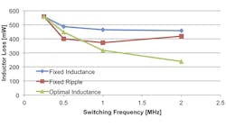
Let’s further investigate the size and loss advantages that increase switching frequency yields by evaluating DC resistance and core losses over switching frequency (while scaling the inductance value) for a given inductor package size. Fig. 1 shows the loss reduction possible by switching at higher switching frequencies. The baseline is a 250kHz, 48V to 5V converter running at a 5A output current and using a 15µH power inductor. By scaling the inductance value inverse to the square root of the switching frequency, both the DC resistance and inductor’s ripple current drops. This scaling method yields near-optimal power-loss improvements. By cutting power losses in the inductor by over 30 percent at 2 MHz, you can make the power stage smaller by using a more compact inductor, along with the compact GaN power module, thus reducing the size of the whole solution.
Higher-Voltage Benefits
You often hear that GaN is superior over silicon, both at high-frequency operation and at higher voltages. Let’s attempt to validate that claim through the construction and evaluation of a hard-switching figure of merit (FoM). The FoM will consider gate-power loss, output-capacitance power loss and reverse-recovery loss during each switching cycle due to transistor switching, as normalized by the device RDS(ON) and its voltage rating.
In a synchronous buck converter operating at high load currents, the output-capacitance loss and reverse-recovery loss occur on one switching edge per period, whereas the inductor current provides zero-voltage switching on the other edge. You can calculate the hard-switching FoM of a FET as:

Where:
RDS(ON) = FET on-state resistance
QG = Total gate charge in nC
QOSS = Output charge in nC
QRR = Reverse-recovery charge in nC
VG = Gate Voltage
VDS = Drain-source voltage
The FET’s output charge (QOSS), rather than the output energy (EOSS), reflects the switching energy loss due to both devices in the half bridge, due to both devices being charged in series from the DC bus voltage.
The units of the FoM are seconds; you can loosely interpret this as the frequency performance of a buck power stage. Lower numbers mean that the power stage supports higher switching frequencies.
Fig. 2 shows the hard-switching metric for a number of silicon and GaN devices rated between 25 V and 100 V. The low-voltage transistors here would be suitable for 12V buck converters, while the higher-voltage transistors are suitable for 48V converters. GaN transistors show a significant advantage over their silicon brethren, primarily due to the lack of reverse-recovery effects. Even when using low reverse-recovery transistors, GaN still has a three-times better FoM. At high voltages, silicon transistors become much worse, but GaN transistors maintain similar performance. This FoM comparison shows that at high voltages and high switching frequencies, the reverse-recovery charge and other characteristics of silicon FETs contribute excessively large losses, further advocating for the use of GaN.

Experimental Comparison
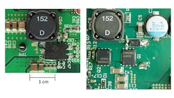
To validate the advantages of GaN presented in this paper, we evaluated buck converters based on the LMG5200 80V GaN half-bridge module, and a buck converter built using state-of-the-art silicon FETs.2 The GaN module uses 18mΩ transistors, while the silicon converter uses 100V, 34mΩ super-junction silicon FETs. We chose a larger RDS(ON) MOSFET to optimize the efficiency of the silicon-based converter by reducing switching losses. We set both converters to operate at 2.2 MHz, modifying them to use identical power-stage inductors. Fig. 3 shows the power stages of both converters. Given the integration offered by the GaN module, the GaN converter offers a more compact form factor. As silicon FETs have a significant reverse-recovery charge, we used a Schottky diode in parallel with the low-side FET to reduce the effects of QRR.
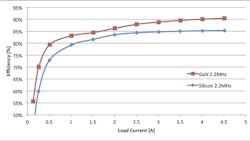
While size is important in these buck converters, so is efficiency. As switching losses often dominate converters operating at 48V and over 1 MHz, GaN should exhibit substantial benefits here. Fig. 4 shows the efficiency of both converters over load. The GaN-based converter attains 90 percent efficiency at peak load, while the silicon-based converter achieves only 85 percent efficiency. We ran each converter until the case temperature of the power device reached 25°C under the rated junction temperature with airflow. Despite the LMG5200’s smaller form factor, it was capable of the same power output as the silicon-based converter because of its higher efficiency.
GaN transistors, through their reduced input and output charge and zero reverse-recovery charge, are capable of simultaneously operating at higher switching frequencies and voltages. GaN can deliver significant advantages over traditional solutions in the industrial, automotive and telecommunications spaces, with voltage buses around 48 V.
Investigating the efficiency and solution-size benefits of operating at high frequencies revealed substantial advantages when operating around 2 MHz. Constructing a hard-switching FoM showed the fundamental advantages of GaN while switching at high frequencies, while a 48V to 12V buck converter illustrated the significant size and performance advantages GaN offers at this frequency range.
References
- Mehta, Narendra. GaN FET module performance advantage over silicon. Texas Instruments, March 2015.
- 80-V, GaN Half-Bridge Power Stage. LMG5200 data sheet, Texas Instruments, March 2015.
The authors may be contacted at:
Comment About the Article
To join the conversation, and become an exclusive member of Electronic Design, create an account today!

Leaders relevant to this article: