The Future Favors UFS for High-Performance Embedded Flash
What you'll learn:
- How SLC, MLC, and TLC technologies affect density, cost, and endurance.
- The distinction between raw NAND and managed NAND like eMMC and UFS.
- Why many future designs will favor UFS over eMMC.
Flash memory is so pervasive today that it’s easy to overlook until it becomes a bottleneck. It stores everything from the firmware in a microcontroller-based IoT device to the data feeding AI accelerators in data centers. For decades, NAND flash has been scaling up in density and scaling down in cost, enabling entire product categories from consumer-grade devices on out, including SSDs, USB drives, memory cards, smartphones, and cloud storage.
The technology traces back to 1987, when Toshiba — now operating its memory business as KIOXIA — introduced NAND flash as a high-density alternative to NOR. Since then, NAND flash has evolved into a full stack of cell architectures, controllers, and host interfaces, with each new generation geared for higher capacity and throughput.
But the memory itself is only part of the puzzle. Understanding the differences between unmanaged and managed NAND is critical when it comes to designing embedded systems that must remain in the field for as long as a decade — or more.
At the interface level, the long-dominant embedded MultiMediaCard (eMMC) standard is increasingly being replaced by Universal Flash Storage (UFS), which comes with a serial architecture that allows for higher bandwidth and lower latency.
What follows is a look at the fundamentals of flash memory and the technical forces driving the shift to UFS in embedded systems.
What are the Differences Between SLC, MLC, and TLC Flash Memory?
At the cell level, NAND flash memory stores information as discrete charge levels. The number of bits per cell determines the number of voltage levels that must be resolved:
- SLC (single-level cell): 1 bit per cell (2 levels)
- MLC (multi-level cell): 2 bits per cell (4 levels)
- TLC (triple-level cell): 3 bits per cell (8 levels)
- QLC (quadruple-level cell): 4-bit-per-cell, now sampling
Unmanaged SLC is the fastest and most robust form of flash storage, but it’s typically only offered in low densities. MLC and TLC increase the storage capacity by encoding more bits per cell, but the tradeoff is that they require more sophisticated sensing, error correction, and management, which creates overhead for the host processor in the system.
Today, most high-volume applications use 3D TLC flash as it delivers the best balance of density, cost, and endurance for modern applications.
Unmanaged vs. Managed NAND: The Difference is in the Flash Controller
Flash memory is available in two forms: unmanaged — or “raw” in industry parlance — and managed.
In the case of raw NAND, memory suppliers can place one to 16 raw NAND die into a single package. The host processor in the system or an external flash controller must handle tasks like error-correction coding (ECC), wear leveling, bad block management, logical-to-physical mapping, and garbage collection.
While this gives OEMs maximum flexibility, it also leaves them with maximum responsibility. Creating a robust flash translation layer (FTL) is a non-trivial task, especially as flash geometry and endurance constraints continue to evolve.
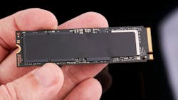
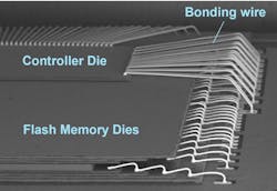
In contrast, managed NAND combines one or more flash die with a dedicated controller in the same package (Fig. 1). The internal controller abstracts the complexity, exposing a simple block-device interface to the host. NAND flash benefits enormously from management, hence, the electronics industry’s broader shift to managed flash.
Managed flash is available in two widely adopted interface standards: eMMC and UFS. These standards allow designers to avoid low-level flash management altogether and focus their attention on system-level functionality.
What is eMMC? How the Standard Solved Embedded Storage Fragmentation
In the early 2000s, mobile devices were caught in a tangle of incompatible NAND interfaces, vendor-specific commands, and custom controllers. Every new handset required new drivers, new boot code, and often new hardware.
The electronics industry desperately needed a unified command set, predictable managed behavior, drop-in replaceability across vendors, and a simplified, block-device view of storage. The MMC Association and JEDEC responded by plotting out the eMMC standard.
The first iteration of eMMC appeared in 2006. The industry consolidated around it fast. By 2010, it had become the dominant storage interface for embedded flash used in smartphones, tablets, and other consumer electronics.
eMMC delivered what the market urgently needed: simplicity, standardization, and predictable behavior.
What is UFS? Why the Standard is Replacing eMMC in High-Performance Systems
But as smartphones started capturing more video, running richer operating systems, and handling larger applications (and more of them at once), eMMC started to run out of performance. Its parallel, half-duplex interface enables either a read or a write operation at one time, but not both. Even at its fastest, eMMC tops out at around 400 MB/s of peak throughput, creating a bottleneck in data-intensive, multitasking environments.
To address this, JEDEC introduced UFS in 2011 as the presumptive successor to eMMC. Instead of a parallel bus, UFS uses a high-speed serial interface (Fig. 2). The result is a point-to-point connection that supports full-duplex communication — simultaneous reads and writes — along with lower latency and more efficient command handling.
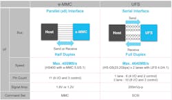
The performance gap between the latest generations of eMMC and UPS is significant:
- eMMC: 400 MB/s of peak throughput
- UFS: up to 4,640 MB/s
That’s more than a 10X improvement, and along with the lower latency and other advantages, it also comes with significantly improved energy efficiency per bit transferred. These features make UFS not just faster, but better suited for sustained data-heavy workloads in today’s mobile and embedded systems. These include high-resolution imaging, augmented reality (AR), AI acceleration, 5G applications, and multi-gigabyte data transfers.
Why eMMC Still Matters: Cost and Longevity for Embedded Systems
Given the vast performance disparities, many expected eMMC to disappear and be completely replaced by UPS. That hasn’t happened. Embedded designers still choose eMMC for applications like printers, set-top boxes, home IoT hubs, streaming devices, low-end mobile devices, and systems using older processors that lack UFS interfaces. In these markets, performance isn’t the priority. Cost and simplicity matter more.
However, the type of NAND used in eMMC is changing. Low-density eMMC parts with 4-, 8-, and 16-GB densities were primarily built with MLC NAND. But MLC manufacturing capacity is rapidly vanishing as the memory industry has fully embraced 3D TLC. As a result, more advanced lithography equipment for MLC simply isn’t being built anymore. As low-density MLC-based eMMC becomes scarce, TLC-based eMMC memory is staying around to replace it.
The practical capacity floor must rise. Moving forward, 64- and 128-GB TLC eMMC parts will be mainstream, while 256-GB parts are available from some vendors, particularly for automotive. This creates an interesting convergence point: the high end of eMMC capacity now overlaps the low end of UFS.
Choosing Between eMMC and UFS: What Really Drives the Decision
When memory vendors consult with customers, a few consistent themes arise when it comes to choosing between these technologies:
- Processor interface compatibility: Many legacy processors only support eMMC, while numerous modern SoCs support only UFS. Some mid-range parts support both. Over time, processor vendors have been phasing out eMMC interfaces in new designs, leaving companies that are upgrading the processor in their system to default to UFS.
- Application class: Broadly speaking, UFS dominates in smartphones, tablets, AR/VR, automotive ADAS, drones, robotics, security cameras, factory automation, and emerging AI-edge platforms. Meanwhile, eMMC persists in printers, set-top boxes, low-cost IoT, media streamers, and older embedded designs.
- Capacity trends: As applications need more storage, and as low-density MLC disappears, designers selecting 64-or 128-GB parts today find themselves standing on UFS’s doorstep.
- Performance: Every customer acknowledges that UFS is superior in throughput, latency, and scalability. Resistance usually comes down to: “My SoC doesn’t support UFS.”
Why UFS is Becoming the Default for Next-Generation Embedded Flash
For now, there remains a healthy market for both eMMC and UFS. eMMC continues to serve cost-sensitive, long-lifecycle, and legacy applications well. Vendors will support mainstream capacities (64 and 128 GB) for years to come.
But the industry trajectory is unmistakable. Low-density eMMC is disappearing, MLC production is nearly gone, processor vendors are phasing out eMMC support, and UFS capacity, performance, and ecosystem momentum continue to grow. In smartphones, tablets, and PCs, markets that once relied exclusively on eMMC, the future roadmap points squarely toward UFS-only designs.
For new system designs, engineers would be wise to consider this direction. While eMMC will not vanish overnight, UFS is increasingly the mainstream, future-proof choice for embedded storage.
About the Author

Isabelle Evans
Director Business Development, Managed Flash Consumer Product, KIOXIA America
Isabelle Evans is the Director of Business Development for Managed Flash Memory at KIOXIA America. She began her career with KIOXIA (then Toshiba America) in 1984 and managed a broad range of memory solutions including PSRAM, SRAM, and NOR flash. She was one of the first to introduce NAND Flash to the market back in 1997. She has been key to the development and sustainability of managed flash-memory products.
Isabelle holds a Bachelor of Science in Business and Marketing degree from the University of Phoenix.
Comment About the Article
To join the conversation, and become an exclusive member of Electronic Design, create an account today!

Leaders relevant to this article: