Between the Lines: The Next Frontier in 3D NAND Flash
What you'll learn:
Since its introduction into the memory market in the late 1980s, NAND flash has fundamentally changed how large amounts of data are stored and retrieved.
Engineered for high-density data storage, this non-volatile memory is present in virtually every segment of the electronics market, from smartphones to data centers and everything in between. It’s used in most removable and portable memory devices such as SD cards and USB drives. In recent years, 3D NAND has also played an important role in the AI boom, providing efficient storage for the huge amounts of data needed to train AI models.
As the demand for data storage explodes, chip companies are racing to increase the cell density of NAND flash memory, expressed in terms of gigabits per square millimeter (Gb/mm2), while reducing the cost per bit. More than a decade ago, the semiconductor industry moved from 2D to 3D NAND to overcome the constraints of traditional memory scaling. In recent years, companies are boosting storage density by increasing the number of layers of memory cells per chip and the number of bits stored per cell (up to four in a commercial NAND flash).
Among the most significant developments is the shift from the floating-gate transistor to the charge trap cell. While floating-gate technology stores electric charges in conductors, the charge trap cells store charges in insulators. That reduces the electrostatic coupling between the memory cells, improving read and write performance. The charge trap cells also open the door to higher densities because they can be manufactured smaller than floating gate.
But as 3D NAND increasingly pushes the limits of physics, the semiconductor industry is turning to several new technologies to cram memory cells more tightly together — not only laterally but vertically, too. Several new innovations developed by imec enable vertical scaling without sacrificing the performance and reliability of the memory: airgap integration and charge trap layer separation.
Inside the Charge Trap Cell: The Building Block of 3D NAND
The semiconductor industry is aiming to adopt gate-all-around (GAA) or nanosheet transistors for logic chips in the next several years. But the GAA architecture is already widely used in the world of 3D NAND flash, where it’s the workhorse for high-density data storage. In this 3D architecture, the memory cells are stacked to form a vertical string, and the cells are addressed by horizontal word-lines.
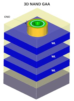
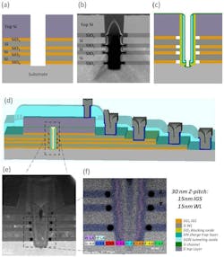
In most cases, the charge trap cell acts as the storage device in 3D NAND. The memory cell resembles a MOSFET. However, it adds a thin sheet of silicon nitride (SiN) embedded inside the transistor’s gate oxide. That turns the gate oxide into a stack of semiconductor material called the oxide-nitride-oxide (ONO) stack, with the layers acting as the blocking oxide, trapping nitride, and tunnel oxide, respectively (Fig. 1).
When the gate is biased positively, electrons from the channel region tunnel through the layer of silicon oxide and are trapped in the SiN layer. That raises the threshold voltage of the transistor. The state of the cell can be measured by applying a voltage from the source to the drain. If current flows, that means no electrons are trapped, and the memory cell is in a state representing a “1.” If no current is measured, the cell is in what’s called the “trapped electrons” state, which corresponds to a “0.”
The charge trap cell is implemented in the 3D NAND structure using a GAA vertical channel method. Imagine rotating the planar transistor over 90 degrees, with the now-vertical conduction channel surrounded by the gate stack.
Download the PDF of this article, and check out our coverage of the Future of Storage and Memory Conference 2025

The manufacturing process for the GAA channel starts by stacking alternating layers of conductor (silicon, to serve as the word-lines) and insulator (silicon oxide, to separate the word-lines). Next, cylindrical holes are formed by drilling down through the stack using advanced dry etching tools. Finally, alternating layers of silicon oxide and SiN are deposited on the sidewalls of the hole, with the polysilicon transistor channel at the center of it all. This arrangement is often referred to as the macaroni channel.
The Next Generation of 3D NAND: Cell Stacking and Cell Scaling
In the years to come, the memory industry will push the GAA-based 3D NAND flash roadmap to its ultimate limits.
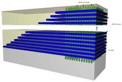
Today, major players are rolling out 3D NAND flash chips with over 300 oxide/word-line layers stacked on top of each other (Fig. 2). This number will further increase, with 1,000 layers projected by 2030, translating to approximately 100 Gbit/mm2. The challenge is keeping the string about the same diameter through the 30-µm-thick stack. But keeping everything uniform in such a small space induces ever higher processing complexity and cost, challenging the tall stack deposition and high-aspect-ratio etch steps.
To supplement the stacking of more layers, semiconductor companies are investing in several complementary tools to increase the storage density of 3D NAND. These “scaling boosters” include increasing the number of bits per cell and reducing the x-y pitch of the GAA cell (lateral scaling). In addition to these improvements in bit and cell density, companies are also taking steps to enhance the area efficiency of the memory array.
One of the other scaling boosters is tier stacking, in which flash memory devices are stacked on top of each other to increase the total number of layers. In 3D NAND, the cells are series-connected to form a string, which is accomplished by stacking alternating layers of insulator and conductor and drilling a hole through them. The process of cell stacking can be repeated two or three times — potentially four times in the future — to create even longer strings per chip. Each stack of cells is sometimes referred to as a “tier.”
By slicing up massive stacks of memory cells and placing the tiers on top of each other to create a taller 3D NAND chip, companies can increase the total number of layers without having to manufacture them all at the same time. For instance, companies can assemble 250 layers of memory cells and then stack four of these tiers into a single 3D NAND chip with 1,000 layers. The main challenges are etching deep-enough holes through these multi-story memory chips and then filling them uniformly.
On top of that, companies are detaching the underlying logic from the NAND array and reattaching it in a configuration called CMOS-bonded-to-Array (CbA). In this arrangement, the CMOS is manufactured on a separate silicon wafer and then attached to the NAND array using advanced packaging, specifically hybrid bonding. CbA is the next evolutionary stage of CMOS-under-Array (CuA), where the NAND is manufactured on top of the CMOS as part of the same monolithic process.
Looking ahead, companies are contemplating bonding several memory arrays on top of a single CMOS wafer as an alternative method of tier stacking — and even multiple array wafers to multiple CMOS.
To control the rising manufacturing costs, imec and others in the semiconductor industry are also pursuing vertical or “z-pitch” scaling, which reduces the thickness of the oxide and word-line layers. As a result, more memory layers can be stacked at a manageable cost.
The Pros and Cons of Z-Pitch Scaling for 3D NAND Flash
Shrinking the space between memory layers is critical to continue driving down the cost of next-generation 3D NAND. The pitch between adjacent word-lines is approximately 40 nm, and the point of z-pitch scaling is to further reduce the thickness of both word-line and silicon-oxide layers in the stack. That allows adding more layers — and hence, memory cells — for every micrometer of stack height, providing a cost benefit.
However, without optimizations, z-pitch scaling can negatively impact the electrical performance of memory cells. It may result in threshold voltage reduction, enhanced sub-threshold swing, and decreased retention. In addition, it can increase the voltages used to program and erase data stored in memory cells, which inevitably increases power consumption, reduces the speed (RC delay) of the memory cell, and could lead to dielectric breakdown of the inter-gate dielectric between adjacent cells.
These effects can be traced to two physical phenomena that become more dominant when squeezing the memory cells closer together: cell-to-cell interference and lateral charge migration.
When reducing the thickness of the word-line layer, the gate length of the charge trap transistor shrinks accordingly. As a result, the gate increasingly loses control over the channel, facilitating electrostatic coupling between different cells.
In addition to cell-to-cell interference, the shrinking of the memory cells in the vertical direction leads to lateral charge migration (or vertical charge loss): Charges trapped inside the memory cell tend to migrate out of the vertical SiN layer, compromising the retention.
Charge trap cells have two geometrical directions: z and x-y (the x and y dimensions are identical because the cell has cylindrical symmetry). Charges can leak out of the memory cell in both directions. While charges stray out of the cell in the x-y direction through the tunnel and/or blocking oxides in the gate, they can also leave the cell in the z direction, ending up inside or too close to the adjacent cell. That happens due to lateral charge migration, which becomes more important as the cells are scaled vertically and get closer to each other.
Next, we discuss the technology enablers that can address these drawbacks, allowing researchers to unlock z-pitch scaling for future generations of 3D NAND flash.
Between the Lines: Integrating Airgaps to Reduce Cell Interference
Integrating airgaps between adjacent word-lines is one potential solution to the issue of cell-to-cell interference. These airgaps have a lower dielectric constant than the inter-gate dielectric, reducing the electrostatic coupling between memory cells. It’s a trick that was widely used in planar 2D NAND flash architectures. But integrating airgaps into the tall silicon-oxide/word-line stack is significantly more challenging.
To overcome these complexities, imec presented a unique integration scheme at the 2025 IEEE International Memory Workshop (IMW) that carefully controls the placement of airgaps between the word-lines.1
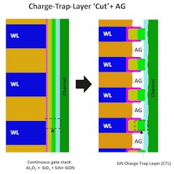
In 3D NAND, thin sheets of silicon oxide are placed both inside the gate of the memory cell—to serve as the “gate dielectric” separating the word-line from the transistor channel—and between the word-lines of different memory cells—to serve as the “inter-gate dielectric” separating adjacent cells from each other (Fig. 3). The gate dielectric forms the tunnel and blocking layers of the ONO stack, and it surrounds the charge trap SiN layer.
As a result, silicon oxide is present not only inside each memory cell, but also between the cells. Due to how the 3D NAND memory cell is manufactured, the gate dielectric runs continuously from cell to cell, and it intersects with the inter-gate dielectric in the space between adjacent memory cells. imec determined that this is the ideal location for placing the airgap. However, it’s a huge challenge to remove (or cut out) the charge trap SiN layer in between the cells with today’s process technology.
At imec, we worked out a new way to integrate the airgap without slicing the SiN out of the memory cell. The innovation introduces the airgap from within the memory-hole region by recessing the inter-gate silicon oxide before depositing the ONO stack. The airgaps are self-aligned to the word-line, allowing for very accurate placement. The approach is also potentially scalable, which was the main issue with other proposed solutions.2
Devices with airgaps were shown to be less sensitive to interference from adjacent cells than devices without them. This was concluded from the smaller shift in threshold voltage measured for devices with airgaps when applying a so-called pass voltage on the unselected gates (Fig. 4). The results were obtained on a test device with limited word-line layers at 30-nm pitch (15-nm gate length and 15-nm silicon-oxide inter-gate dielectric), and memory holes measuring 80 nm in diameter.
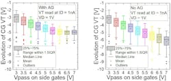
Researchers at imec also investigated the impact of airgaps on memory performance and reliability. The airgaps didn’t affect the memory operation, supporting an endurance of up to 1,000 program/erase cycles, comparable to devices without airgaps.
Based on these results, the hole-side airgap integration is considered a crucial step in enabling future z-pitch scaling.
Charge Trap Cut: Where It Fits into the Future of Flash Memory
It was proven by imec that it’s possible to introduce airgaps in the inter-gate dielectric layer. However, these hollows in the memory cell currently stop before the blocking oxide. What if we could drill even deeper into the memory cell, introducing airgaps to the region of the blocking oxide and charge trap layer?
We tested out the approach in simulations and showed that such a charge trap layer separation (or charge trap cut) can increase the memory window of the cell (Fig. 5). In addition, the charge trap cut can prevent charges trapped in the memory cell from migrating laterally through the SiN string that runs from top to bottom along the height of the oxide/word-line stack.
Data is stored in flash-memory cells by programming the threshold voltage to different levels. To store a single bit, the cell requires two levels: for instance, 0 V and 1 V. To store 2 bits, the cell requires four levels: for instance, 0 V, 0.5 V, 1 V, and 1.5 V. As the number of bits rises, the number of voltage levels also rises.
It’s necessary to increase the total range of threshold voltages (the memory window) or reduce the separation between adjacent levels (1 V of separation when working with 1 bit, 0.5 V with 2 bits). But telling the difference between these voltage levels becomes more difficult when they’re closer together. By increasing the memory window, the charge trap cut could help enable more levels — and thus, more bits — per cell.
But integrating a charge trap cut in 3D NAND flash is a non-trivial task, as it requires directional etching and deposition through the sidewalls of extremely deep and narrow holes. For these structures, the toolbox of technologies used for 2D NAND flash is no longer going to cut it. Currently, imec is working with its suppliers on new techniques that enable this charge trap cut in a controllable way.
Once the charge trap layer can be interrupted, imec intends to combine it with the airgap integration scheme to deliver a complete and scalable solution for the z-pitch scaling challenges.
“Cutting” Through the Complexities of 3D NAND Flash
As the semiconductor industry races to store more data in smaller spaces, the z-pitch scaling of 3D NAND flash is becoming key to managing costs tied to the increasing number of memory layers. Building on its long-standing processing expertise and strong ecosystem of equipment suppliers, imec is developing the key technologies that support aggressive z-pitch scaling while preserving memory operation and reliability: airgap integration and charge trap cut.
At the same time, gains from traditional charge trap cell architectures are starting to slow, and improvements in memory density could taper off before the end of the decade. As a result, researchers are taking a hard look at more radical cell architectures to carry the memory roadmap beyond 2030. One proposed 3D approach reimagines the entire layout, arranging the conduction channels of the memory cells horizontally instead of vertically.3
In another approach, evaluated by imec in 2023, the charge trap memory cells are connected through a trench-based architecture instead of integrating the cells in a circular GAA geometry, potentially delivering a leap in bit storage density.4
All of these developments show that several technologies in the pipeline will allow the memory industry to gradually move to 100 Gb/mm2 of data storage — a demand driven primarily by cloud computing and AI applications.
References
1. “Hole-side airgap integration as enabler for 3D NAND flash z-pitch scaling,” S. Rachidi et al., 2025 IEEE International Memory Workshop (IMW).
2. “A confined storage nitride 3D-NAND cell with WL airgap for cell-to-cell interference reduction and improved program performances,” D. Resnati, 2024 VLSI.
3. “Superior scalability of advanced horizontal channel flash for future generations of 3D Flash memory,” M. Oda, 2024 IEDM.
4. “Imec improves memory window of a 3D trench cell for next-gen NAND Flash,” imec.
Download the PDF of this article, and check out our coverage of the Future of Storage and Memory Conference 2025
About the Author
Sana Rachidi
Senior Integration Researcher, Memory Process Integration Team, imec
Dr. Sana Rachidi received her M.S. degree in material science and surface treatments in 2016 from ENSIL-ENSCI Engineering school and from Limoges University, France. In 2020, she received her Ph.D. in nanoelectronics and nanotechnologies from Grenoble Alpes University UGA, France, where she worked on enabling dry- and wet-etch process developments for beyond 8-nm GAA CMOS.
She joined imec, in Leuven, Belgium, in 2021, where she is currently working as a senior R&D engineer in memory process integration, semiconductor device design for several internal and external projects covering storage and MRAM.
Maarten Rosmeulen
Program Director, Storage Memory Program, imec
Dr. Maarten Rosmeulen received his M.S. degree in physics in 1993 and his M.S. degree in micro-electronics physics and materials science in 1994, both from the KU Leuven, Belgium. In 2005, he received his Ph.D. in electrical engineering from KU Leuven. Since then, he has worked at imec, in Leuven, Belgium, where he has been active as an R&D engineer in process integration, semiconductor device design, and electrical device characterization for multiple internal and external projects.
In 2009, he became a project leader in developing GaN-on-silicon light emitting diodes (LEDs). In 2014, he became the team leader of the pixel design and testing team and has been responsible for the development of CMOS image sensor technologies. In 2019, he became the program director of the storage memory program, the position he holds today.
Comment About the Article
To join the conversation, and become an exclusive member of Electronic Design, create an account today!

Leaders relevant to this article: