Power Shift: Designing GaN into Switch-Mode Power Supplies
This article is part of an Electronic Design special report and the Dostal's Design series.


What you’ll learn:
- The power-handling properties of GaN.
- The unique challenges of using GaN in switch-mode power supplies.
- Upgrading from silicon MOSFETs to GaN power devices.
- How to choose switching controllers and gate-driver ICs for GaN.
- What’s the future for GaN power technology?
Silicon is the most amazing material for electronics. The ability to grow pure bulk silicon and dope for both p- and n-type properties has been a huge boost for the power electronics industry, leading to low-cost, high-performance switches that permeate virtually everything with a battery or a plug.
A Few Comments on GaN from Frederik Dostal
As a result, designers’ experience with building circuits out of silicon is enormous. Their familiarity with it has enabled the industry to push the boundaries of silicon further and further over time. However, while silicon performs well in various applications, certain material traits limit advances in speed, power density, and temperature range—all of which matter to the latest switch-mode power supplies (SMPS). The pressure to seriously consider an alternative technology is increasing the focus on silicon carbide (SiC) and gallium nitride (GaN).
SiC has been used in electronics for a very long time. Early applications involved light-emitting diodes (LEDs). Lately, it’s being used as a power-stage component in power supplies due to its high-temperature and high-voltage capability. Switches and diodes with voltage ranges way above 1,000 V are available.
One other technology that can replace or enhance silicon circuits in power applications is GaN. Widely used for consumer fast-chargers and power adapters, it’s also now gaining relevance in areas such as electric-vehicle (EV) onboard chargers (OBCs) and DC-DC converters, where it’s necessary to handle thousands of watts at a time safely and robustly. GaN also has the potential to alleviate some of the power challenges posed by AI in data centers, weaving its way into the power-supply units (PSUs) in server racks.
GaN is becoming more and more popular for these switch-mode power supplies. For circuit designers interested in using this relatively new technology, it’s necessary to not only understand the benefits and the challenges, but also gain experience with it.
The Power-Handling Properties of GaN
GaN was used for the first time in power switches as a replacement for silicon field-effect transistors (FETs) in SMPS in 2012. These prototype pGaN HEMTs showed higher power-conversion efficiency compared to a standard silicon FET device.
The main difficulty with GaN power technology was—and still is—driving down its cost. The ability to grow large single crystals for manufacturing large, high-quality wafers full of GaN power devices remains a challenge.
Working through these challenges will be worth it. though. GaN comes with a wide range of advantages over silicon when it comes to converting power. The main benefits of GaN power devices are the lower drain and gate capacitance for a given current and voltage rating. In addition, GaN switches are physically smaller than silicon, resulting in a more compact solution.
The material properties of GaN mean that it also has a high breakdown voltage, which is useful in applications running at voltages of 100 V and above. However, below 100 V, the power density and the capability of fast switching can give this technology advantages, such as higher power-conversion efficiency, when designing different power supplies.
GaN is a wide-bandgap (WBG) semiconductor, which means that the bandgap voltage is 3.4 eV versus the 1.1 eV of silicon. However, figures of merit matter differently in power-supply design. A valuable use case would be in 400-V intermediate bus applications, such as in 240-V AC power converters where we use 650-V breakdown voltage FETs with a drain source current of roughly 30 A. This system requires a gate charge of 93 nC when using a silicon FET, versus only 9 nC using a GaN FET. An application utilizing such switches would run in power levels roughly between 1 and 8 kW.
>>Check out these TechXchange for similar articles and videos
The benefit of using the GaN device with the small gate capacitance results in much faster switch transition times and reduced switching losses. Ultimately, it would lead to higher power-conversion efficiency, especially at higher switching frequencies with smaller magnetics.
The Unique Challenges of Using GaN in Switch-Mode Power Supplies
A number of challenges emerge when replacing silicon MOSFETs with GaN power devices. These challenges relate to the requirements for gate drive, fast-changing voltages during switching, and high conduction loss during dead times.
First, GaN switches typically have lower gate voltage ratings than silicon FETs. Most manufacturers of GaN devices recommend a typical gate-drive voltage of 5 V. At the same time, it’s not unusual to have GaN devices with an absolute maximum rating of 6 V, which doesn’t leave much headroom between the recommended gate-drive voltage and the critical threshold, above which the voltage can damage the device. This limitation, along with the fact that the gate charge in GaN devices is so small, means that driver stages must strictly limit the maximum gate-drive voltage to avoid damage to the GaN device.
Second, one must deal with the fast-changing voltages—also called dv/dt—of the power supply’s switch node. These transient voltages may cause false turn-on of the bottom switch. The gate of a GaN device is relatively small. As a result, any fast voltage changes in the vicinity, such as the switch node, may capacitively couple onto the small gate of the GaN switch and turn it on. Gaining more control of the turn-on and turn-off profiles requires a separate pull-up and pull-down pin and a carefully designed PCB layout.
Lastly, GaN FETs have a higher conduction loss during dead times. These are the times when both the high-side and low-side switch of a bridge configuration are turned off. Dead times are necessary to prevent a short circuit from the high-side voltage rail to ground. During the dead time, the low-side switch typically develops current flow through a body diode of the low-side switch, which is what causes the conduction losses.
One way to solve this problem is to strictly minimize the length of these dead times. This needs to be done without generating overlapping times of the high-side and low-side switches, which can cause a short circuit to ground.
One other point to mention is the fact that GaN offers a wider conversion range. The fast rise and fall times provide a smaller duty cycle than with silicon MOSFETs.
Switching It Up: Upgrading From Silicon MOSFETs to GaN Power Devices
For many years, silicon has formed the backbone of the power-conversion industry. Now that GaN switches are available for power-supply designers, the question is, “Are they simply a drop-in replacement or do you have to redesign the power stage around them?”
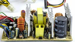
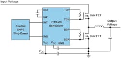
Figure 1 shows a power stage in a typical buck-regulator SMPS. The red arrows indicate additional components that may be necessary when using GaN switches in a SMPS.
Unlike silicon MOSFETs, GaN switches don’t have a body diode—they have a different mechanism to yield similar results. Only majority carriers are involved in GaN device conduction, so there’s zero reverse-recovery charge (Qrr). However, the GaN FET doesn’t have the forward voltage of the body diode, as with silicon MOSFETs, so the voltage across the GaN FET may get quite large. Thus, the power losses during the dead time are quite high. This is why it’s important to reduce the dead time when using GaN switches compared to silicon switches.
Power designs use a silicon MOSFET’s body diode excessively during the dead time in a SMPS. In a buck regulator’s low-side switch, the current flow through its body diode provides the continuous current flow demanded by the inductor. Without a body diode in the low-side switch, every bit of dead time would cause the switch node in a buck regulator to go to minus infinity voltage. Most certainly the circuit would lose energy and eventually blow up due to voltages outside of the rated voltage of the switch, before reaching minus infinity.
If the source and gate are at the same potential when using a GaN switch, but with a continuous current source such as the inductor, the GaN FET will turn on in reverse.
Since GaN switches don’t include a p-n junction body diode, the low-side switch needs to be constructed with an alternate current path around the low-side switch, allowing for current flow during the dead time. Figure 1 shows a simple Schottky diode (D2) placed between drain and source of the low-side GaN switch. This diode will quickly take over the inductor current flow during the dead time of the circuit.
During the reverse conduction, the drain and the source get flipped due to the symmetry of the GaN power FETs. The gate remains at ground potential, but the switch node is self-biased to be the minimum turn-on threshold of the GaN FET. This low voltage is the minimum threshold needed to turn the GaN FET on (typically GND-2V to GND-3V). Since the VGS isn’t optimized, the RON suffers during reverse conduction. The external Schottky is an alternative path without turning the GaN FET on in the reverse conduction.
The second modification to the circuit when using GaN switches is the resistor in series with diode D1 (Fig. 2). The resistor is used to supply the voltage to the high-side driver of the circuit coming from the INTVCC supply voltage. The resistor may also be needed to limit peak currents for the high-side driver.

Lastly, the Zener diode (D3) may be needed to prevent voltage spikes from becoming excessive on the high-side driver voltage supply.
While the additional components in Figure 1 look relatively simple and straightforward, ensuring that such a circuit will run reliably in all operating conditions, they require fine-tuning and thorough evaluations on the test bench. Also, variations of component values over production and over aging will need to be considered. The ultimate risk is permanent damage to the GaN switches.
How to Choose Switching Controllers and Gate-Driver ICs for GaN
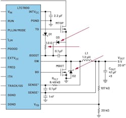
One way to avoid the critical evaluation process of protection functions in a GaN-based power stage of the SMPS is to use a power-supply controller IC specifically designed for GaN. Selecting a dedicated controller makes a GaN power-supply design simple and robust. All the challenges mentioned earlier are addressed and solved with such controllers. Figure 1 shows the simplicity of a step-down power design using GaN FETs controlled by the LTC7891, a single-phase buck controller designed for GaN FETs.
These switching controllers also offer the flexibility needed to work with the different GaN switches on the market today. GaN power technology is far from having finished its path of development and innovation. Though future GaN switches will bring better performance to the table, they may require slightly different handling compared to the switches that are readily available today.
Devices such as the LTC7891 in Figure 2 offer a dedicated up and down gate-drive pin for both switches. With this, the rising and falling slope of the gate voltage of the GaN switches can be controlled separately. It allows for driving the power stage with GaN switches that have minimal ringing and overshoots.
Compared to a standard silicon MOSFET buck controller, the LTC7891 also features separate gate-drive pins for rising and falling edges (Fig. 2, again). However, many other differences separate the LTC7891 from existing controllers designed for silicon switches. There’s an internal bootstrap switch to prevent the overcharging of the high-side driver during dead times. It’s implemented reliably without the need for external components.
Another important feature is very fast dead-time control. It leads to reliable operation and yields significant power-conversion efficiency improvements, while also allowing for high switching frequencies. The LTC7891 is rated for switching frequencies of up to 3 MHz. One other unique feature is the possibility of accurately adjusting the gate-drive voltage from 4 to 5.5 V. This optimizes the VGS needed for various GaN FETs available in the market.
Using passive components with a standard silicon controller, or implementing a dedicated GaN controller, are both viable options. But engineers can also consider using a standard controller IC and adopting a driver stage optimized for GaN. This can also take care of the challenges with GaN and allows for a simple and robust design.
Figure 3 shows the power stage of a buck regulator implemented with the LT8418 driver IC. The driver comes in a very small wafer-level chip-scale package (WLCSP) that enables very low parasitic resistances and inductances for low-voltage offsets resulting from fast current changes.
Once suitable hardware, controller ICs, and GaN switches have been selected, a great way to get first evaluation results is to use a detailed circuit simulation. LTspice from Analog Devices offers complete circuit models that may be used for simulation. It offers a convenient way to learn about using GaN switches. Figure 4 shows a simulation schematic of the LTC7891. A dual-channel version, the LTC7890, is also available.

While GaN technology is brilliant for building FETs and using them in an advanced power stage, GaN isn’t necessarily able, nor cost-effective enough, to be used in the control circuitry for a switch-mode power supply. Therefore, we will see a hybrid approach for the foreseeable future.
The controller will be silicon-based with highly optimized control and drive circuitry to drive a high-power GaN switch. This approach is technologically available today and it’s cost competitive. However, it will require the use of multiple die in one circuit. This entails either having the GaN switches separate, as shown in this article, or by incorporating multiple die in a fully integrated power-converter IC or a µModule power-supply solution that integrates many of the passive components, including the inductor.
As noted, growing large, high-quality GaN wafers remains a challenge. Since around 2010, the mainstream choice in GaN manufacturing is high electron mobility transistors (HEMTs) on silicon due to the larger possible wafer diameters and lower cost associated with existing silicon processing infrastructure.
Early technical challenges with this approach have been resolved. Still, the technology requires years of further development. Instead of being grown as bulk crystals like silicon and SiC, GaN devices are built using GaN epitaxy on silicon wafers. GaN-on-diamond is one potential way of processing GaN switches in the future.
What’s the Future for GaN Power Technology?
GaN has reached a solid point in its development where many SMPS can be designed with it. However, there will be further development with each new generation of GaN switches. The existing SMPS controllers and drivers for GaN from ADI are a flexible and dependable way to work with GaN FETs from different vendors now and in the future.
We’re actively progressing toward broader adoption of GaN technology. While GaN switches by themselves are quite robust today, it’s evident that more time and development will be necessary for engineers to accept the reliability of the switches. The manufacturing processes of GaN switches will also improve further, increasing yield and reducing defect density, thus reducing the cost and enhancing the reliability of GaN switches.
Expect more and more specific GaN drivers, such as the LT8418, and switching controllers like the LTC7890 and LTC7891 buck controllers, to arrive to simplify the implementation of a GaN-based SMPS.
Currently, the most common GaN device voltage ratings are 100 V and 650 V, which is why the first power supplies using GaN operate within these ranges. But the unique characteristics of GaN—specifically, its small gate charge—can also scale down to lower voltages.
In the future, we will also see GaN used in power supplies with maximum voltages as low as 40 V. At the other end of the spectrum, GaN switches may also scale up to 1,000 V. At such high voltages, the fast-switching speeds of GaN can be a difference maker.
Semiconductor materials that expand the operating range and power density of power supplies will continue to be developed. Silicon was the start of it all, and it’s still the center of the power electronics industry. But GaN is going to play a bigger role in the next 10 to 15 years, too. Everything from EVs to AI data centers requires more power, higher density, greater robustness, and higher efficiency. GaN provides the opportunity to keep pace with these innovations.
Read more articles from this special report

>>Check out these TechXchange for similar articles and videos
About the Author

Frederik Dostal
Power-Management Technical Expert
Frederik Dostal is a power-management expert with more than 20 years of experience in this industry. After his studies of microelectronics at the University of Erlangen, Germany, he joined National Semiconductor in 2001, where he worked as a field applications engineer, gaining a lot of experience in implementing power-management solutions in customer projects. During his time at National, he also spent four years in Phoenix, Arizona (USA), working on switch-mode power supplies as an applications engineer.
In 2009, he joined Analog Devices, where since then he held a variety of positions working for the product line and European technical support, and currently brings in his broad design and application knowledge as a power-management expert. Frederik works in the ADI office in Munich, Germany.
Also check out my:
Comment About the Article
To join the conversation, and become an exclusive member of Electronic Design, create an account today!

Leaders relevant to this article: