Measuring High-Frequency Noise in Buck-Regulator Output-Voltage Ripple
What you'll learn:
- Why high di/dt in a buck-converter hot loop can appear as high-frequency VOUT ripple.
- How probe orientation and loop area alter ripple measurements.
- How shielding and low-loop probing reveal the actual ripple at COUT.
In many applications, a switch-mode power supply (SMPS) is the only choice because of its excellent performance, including high efficiency and high power capability. A buck step-down power converter is the most popular topology adopted in a variety of applications. The switching characteristics controlled by pulse-width modulation (PWM) help to regulate power transfer.
At the same time, though, the fast switching transients of power FETs within several nanoseconds or tens of nanoseconds could induce high-frequency noises. For example, in noise-sensitive applications, if the high-frequency voltage spikes caused by the power supply are aligned with the clock signal, it will cause failure or malfunction of the load devices, such as ADCs, ASICs, or FPGAs.
Therefore, it’s important to understand the root causes of high-frequency noises, identify the noise issues, and then find the potential solution to attenuate or eliminate the influence of high-frequency noises. The correct noise/ripple measurement method is critical.
Typical VOUT Ripple in a Buck Converter
For a typical buck converter, the inductor and the capacitor work as a filter to provide the conductive path for the AC signal generated by the switching action. The inductor current contains the AC component and the DC component. Most of the AC components will flow into the output capacitor, and the DC component will only flow into the load.
Without considering component parasitics (Fig. 1a), the output-voltage ripple across the output capacitor is a smooth waveform (Fig. 1b).
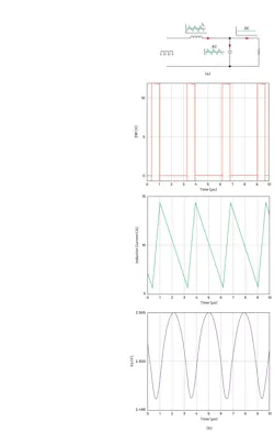
If considering the parasitic resistance and the parasitic inductance of the output capacitors (Fig. 2a), the output voltage ripple could change significantly (Fig. 2b).
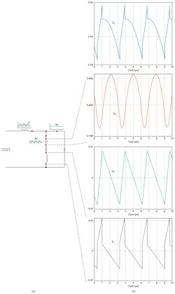
The AC components of the waveform in Figure 2b are mainly distributed around the switching frequency, which is around hundreds of kHz to several MHz. But the actual output voltage in the test will usually show some even higher-frequency components, which are around hundreds of MHz. The parasitic capacitor of the power inductor could provide the conductive path for these hundreds of MHz signals from the switching node to the output (Fig. 3).
Output-Voltage Measurement Example
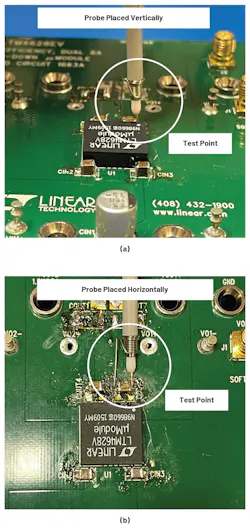
An example of the output-voltage measurement based on the LTM4628 µModule buck regulator is shown in Figure 4a. The switching frequency waveform and the high-frequency spikes can be easily observed. But when changing the position of the probe from vertical to horizontal to the board, the measured output-voltage ripple reduced from 54 to 42 mV (Fig. 4b).
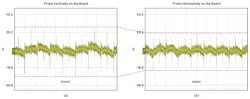
Figure 5 illustrates how the output voltage is measured. If only considering the output-voltage ripple generated on the conductive path, the measurement result should not change with the probe position. Meanwhile, the high-frequency noise captured by the probe is aligned with the switching actions. So, the additional high-frequency noise captured by the probe could be the radiation noise induced by high di/dt in the hot loop during the fast switching transient.
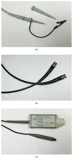
To further verify the presence of these differences caused by the probe position, the different probes are applied to measure the output-voltage ripple, including a general probe, a BNC cable, and an active differential probe (Fig. 6). As shown in the figure, the general probe needs the extra spring as the ground return path, which means the measurement loop is larger.
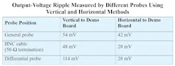
The measurement results with different probes are provided in the table. Compared with the vertical probe measurement, the horizontal probe measurement always shows the lower high-frequency spike. Also, the measurement result of the horizontal method based on the general probe is higher than the BNC cable and the differential probe.
Applying Maxwell Simulation
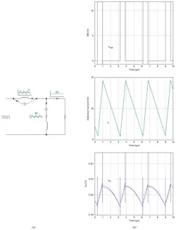
To understand the unexpected phenomena during the output-voltage ripple measurement, the Maxwell simulation model is developed as shown in Figure 7a, based on the simplified LTM4628 physical structure. Hot loop 1 is formed by the MOSFETs and the internal input capacitors inside the module. Hot loop 2 is composed of the MOSFETs and the external input capacitors near the module on the demo board. The conceptual currents at 300 MHz are injected into both hot loop 1 and hot loop 2 to emulate the high di/dt in the hot loop during the switching transient.
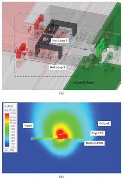
Figure 7b shows the H-field distribution around the module. The H field is much stronger in the module surrounding the area on the top of the demo board. This indicates the flux generated by the hot loop could be easily captured by the probe measurement loop.
As for the root cause of the different results by different probe positions, Figure 8 provides the zoomed-in H-field distribution for a more detailed explanation. Here, the equivalent vertical measurement loop surface can capture around 8X more flux than the horizontal measurement loop surface. This is because the demo board with a thick copper polygon provides the attenuation to the high-frequency flux to prevent the flux from going through. Thus, most of the flux will flow horizontally along the demo board surface.
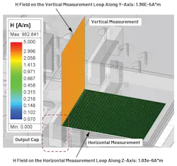
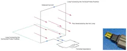
Figure 9 shows a more straightforward illustration of how the vertical measurement loop captures more flux generated by the hot loop. The positive tip, the negative or ground tip, and the return path inside the probe form a loop like an antenna that could capture the high-frequency flux surrounding the switching regulators.
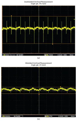
To further verify this concept, the same probe with the shielding is also used to measure the VOUT ripple (Fig. 10). A copper foil is manually rotated around the differential probe to form a shielding layer. The probe is also vertical to the demo board.
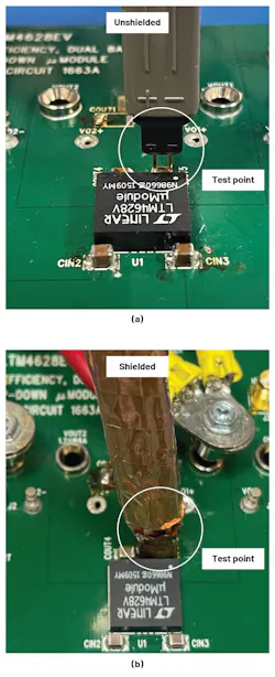
As a result, with the shielded probe, the high-frequency noise is much reduced (Fig. 11) for that in Figure 10b compared with the unshielded measurement in Figure 10a. Except for the high-frequency noise, the switching frequency ripples in both figures are quite similar. Also, as discussed based on Figure 3, there will be high-frequency ripple across the output capacitor because of the parasitic capacitor of the inductor like the waveform in Figure 10b.
Conclusion
The fast switching transient induces the high di/dt in the hot loop. For the output-voltage ripple of a buck converter, there will be high-frequency noise caused by this high di/dt through the conductive path formed by the parasitic capacitor of the inductor.
But in the real VOUT ripple measurement, there will be even higher frequency noise captured, which is aligned with the switching actions as well. This extra ripple is the radiation noise that’s also caused by the high di/dt in the hot loop. And the high-frequency spike can vary with the position of the probe on the demo board. The ANSYS simulation proves that the vertical measurement configuration can capture much higher-frequency flux generated by the hot loop than the horizontal configuration.
To further verify this theory, the VOUT ripple is also measured by the shielded probe. The high-frequency noise is much reduced by the shielded probe than the non-shielded probe result — it turns out there will be additional radiational high-frequency noise captured by the probe. The real VOUT ripple presenting across the COUT on the board will be smaller than the VOUT ripple measured by the probes.
>>Download the PDF of this article, and check out the TechXchanges for similarly themed articles and videos


About the Author
Yu Yan
Staff Applications Engineer, Analog Devices Inc.
Yu Yan received his Ph.D. in electrical engineering from the University of Tennessee. He joined Analog Devices in 2022 as an applications engineer. His expertise includes DC-DC converters, AC-DC converters, and digital control. He worked on the design of electric-vehicle chargers at university and the development of power modules at ADI.
Comment About the Article
To join the conversation, and become an exclusive member of Electronic Design, create an account today!

Leaders relevant to this article: