What’s the Difference Between Lateral and Vertical Power Delivery?
What you'll learn:
- Why traditional lateral power delivery (LPD) breaks down when it comes to AI accelerators that consume more than 1,000 W apiece.
- How vertical power delivery (VPD) addresses the excessive power losses, space limits, and scaling complexity prevalent in LPD.
- How innovations in voltage regulator modules (VRMs) enable VPD to meet the extreme current and density demands of modern AI chips.
Powering a 1,000-A AI accelerator core that runs on less than 1 V is one of the hardest engineering problems faced by power designers today. However, this represents just the beginning of the challenge. Around the main AI accelerator core, there are 40 to 50 secondary power rails for every single primary power rail. These secondary power rails supply power for memory, I/O, and other important functions.
The power distribution network (PDN) for the entire system poses significant difficulties. As current is forced through the resistance present in this network, power losses inevitably add up. These I2R losses can waste more than 20% of the processor’s thermal design power (TDP). When power losses are this high, the traditional lateral power delivery (LPD), where the DC-DC converters sit next to the processor on the same side of the PCB, reaches its limits.
Vertical power delivery (VPD), where the DC-DC converters sit below the processor on the backside of the PCB, is emerging as a solution — not only to feed the primary power rails in the SoC, but also the secondary power rails. Below, we dive into the details of the VPD architecture and how it could help solve the most important constraints of efficiency, space, and scalability in the realm of AI power delivery.
Unpacking the Power Delivery Challenges of Modern AI Chips
The latest AI processors now expend in excess of 1,000 W per chip. In data centers, power requirements are climbing to more than 20 kW per server, with even higher densities being driven by insatiable demands of hyperscalers. Current requirements have surged beyond 1,200 A at increasingly lower voltages. These parameters have created a perfect storm, leading to physical constraints that limit system performance and efficiency.
>>Download the PDF of this article
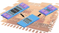
The evolution of AI accelerators (Fig. 1) shows that each new generation demands more power while requiring higher current density.

This leads to three fundamental challenges, each coming with a handful of sub-challenges:
The efficiency problem
When power moves from the PCB to the point-of-load (POL), I2R power loss occurs in the distribution network, which can waste power and generate heat:
- A 48-V to 1-V conversion means 48X higher current, which means substantially higher I2R losses.
- The distribution loss alone can amount to more than 20% of a processor’s TDP.
- Standard LPD can waste 30% to 40% of power from PCB to POL.
The space problem
Power density in high-performance computing accelerators is already in the 1 A/mm2 range and will likely continue to climb. However, these power needs are hitting physical constraints:
- Inductor size is limited by heat generation and core saturation issues.
- Servers have strict height limits (less than 5 mm between boards).
- Larger components like transformer-based converters don’t fit.
The scalability problem
Delivering high currents requires complex multi-phase converter solutions, which are becoming unmanageable:
- Average current per phase is limited to 40 to 60 A, so more than 20 phases with current sharing are needed for high current demands.
- Each DC-DC converter in a multi-phase configuration requires a relatively large inductor, and that conflicts with the space restrictions of servers.
- Longer traces with higher parasitic inductance cause EMI problems, while voltage overshoots and undershoots can damage the processor.
How Vertical Power Solves the Limits of Lateral Power Delivery
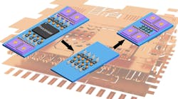
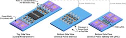
In the standard LPD architecture (Fig. 2), DC-DC converters translate the high-voltage, low-current power from the server’s main power supply to low-voltage, high-current power at the PCB level, which then races into the AI accelerator or other SoC.
The power moves laterally through the distribution network, with the DC-DC converters — also called voltage regulator modules (VRMs) — and accelerators placed side-by-side. This lateral arrangement leads to limited flexibility in board layout. It also consumes a significant amount of board space, which in turn limits system-level density. The heat caused by distribution losses is typically removed by air-, liquid-, or other active-cooling systems. Those take up space, too.
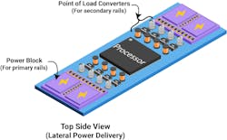
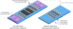
VPD addresses these challenges by delivering power vertically through PCB layers to the processor above, effectively reducing the distance the power travels from the VRM to the system-on-chip (SoC). One method to achieve this is to shorten the secondary power rails by positioning the POL converters on the backside of the PCB directly under the processor (Fig. 3).
By doing so, VPD addresses the three problems of efficiency, space, and scalability in the following ways:
- Efficiency: By converting to the final low voltage closer to where it's needed, the VPD solution shows a 70% reduction in I2R loss and 13.6% system power loss compared to standard LPD. The distribution loss also reduces from more than 20% to less than 7% of ASIC thermal design power.
- Space: VPD moves power delivery components to the PCB backside, which frees valuable board space on the PCB top side and improves form factor. It also frees up PCB space for additional processing, memory, or I/O.
- Scalability: VPD improves scalability by reducing the current routing over longer distances. The high currents can be delivered through multiple compact voltage regulators around the die. It also improves signal isolation, as vertical power helps isolate high-speed signals. In addition, the shorter traces with smaller parasitic inductance minimize EMI problems and voltage overshoots and undershoots, which can damage the processor.
What are the Building Blocks of a Vertical Power Module?
While VPD mitigates many of the power distribution challenges facing AI chips, companies have been reengineering power modules from the inside-out to more effectively support it. For instance, TDK's family of µPOL power modules implement VPD in data centers by reducing the size of POL converters, specifically addressing the secondary power rails, such as memory rails, I/O rails, and SerDes rails.
The underlying architecture is outlined in Figure 4, where the compact, ultra-thin package makes it possible for engineers to place the µPOL module under the PCB. These µPOLs play a complementary role to the "primary power blocks” on the board.
Advanced packaging technologies such as semiconductor-embedded-in-substrate, or SESUB, along with integrated magnetics are key to minimizing the overall size of the module.
SESUB, as shown in Figure 5, helps open the door to VPD by embedding power semiconductors into a chip-embedded package and passive components directly on top of it to minimize parasitic inductance. That eliminates wire bonds and enhances thermal performance thanks to the integration of thermal vias. The arrangement minimizes resistance and inductance, leading to fast response and accurate regulation with dynamic load currents prevalent in AI chips, thus boosting the efficiency of the µPOL.
In addition to minimizing parasitic resistance, capacitance, and inductance that can sap the performance of the DC-DC converter, SESUB reduces package size by 50% to 60% compared to standard solutions. The thermal vias in SESUB dissipate significant heat from the chip to the PCB, with a junction-to-PCB thermal resistance (RθJB) of 1.4 K/W.
One of the latest power modules based on SESUB is TDK’s FS1525 module, which also integrates the power inductors to smooth out current ripples as the µPOL pushes power into the load. The integration helps enable a smaller form factor and better efficiency by reducing parasitics. In this case, the dual-phase design aligns with the interleaved buck approach, and the module can scale from 25 A with a single µPOL up to 200 A using eight µPOLs.
By squeezing everything into a small power module, the DC-DC converter can deliver a power density of 127 A per cubic centimeter. The module implements a more advanced type of modulation called Adaptive on Time (AOT) for ultra-fast transient response with internal loop compensation. Based on a phase-locked loop (PLL), this modulation scheme helps enable 91% and 89% efficiency at 15 A and 25 A, respectively. The I2C and PMBus offer engineers additional telemetry options.
So, what does this mean for power electronics engineers in the AI hardware space? With advanced power modules such as those based on µPOL technology, you can design systems with higher power efficiency, smaller form factors, and better thermal management, addressing the secondary power rail challenges of modern AI and high-performance computing environments.
References
Vertical power delivery for emerging packaging and integration platforms - power conversion and distribution. IEEE Xplore.
A 32-phase 1200-Ampere DC/DC converter for data center and artificial intelligence systems. IEEE Xplore.
Vertical power delivery for 1000 amps Machine Learning ASICs. IEEE Xplore.
Voltage-Stacked Power Delivery Systems: reliability, efficiency, and power management. IEEE Xplore.
>>Download the PDF of this article
About the Author
Bill Pelletier
Senior Field Applications Engineer, TDK Corporation
Bill Pelletier is Senior Field Applications Engineer at TDK Corporation. He's held similar positions at Kinetic Technologies, Monolithic Power Systems, Tyco/Lineage Power, and Sipex.
Comment About the Article
To join the conversation, and become an exclusive member of Electronic Design, create an account today!

Leaders relevant to this article: