Design Scalable Switching Architectures for High-Channel-Count Semiconductor Test Systems
What you'll learn:
- How switching architecture affects semiconductor test system scalability and performance.
- The tradeoffs between selecting reed relays, EMRs, solid-state, and MEMS switching technologies.
- How modular architectures simplify integration, maintenance, and long-term scalability.

The demands placed on automated test systems continue to ramp up in concert with the breakneck speed of semiconductor technology advances. Higher pin counts, rising power requirements, faster interfaces, and growing throughput expectations are forcing engineers to rethink how semiconductor test systems are architected, particularly when it comes to switching.
This is because switching hardware frequently sits at the center of the test platform, connecting instrumentation to the device under test (DUT) and routing signals throughout the system. As channel counts scale into the thousands, the switching architecture’s impact on critical factors such as measurement accuracy, synchronization, throughput, maintainability, and even floor-space utilization grows exponentially.
Traditional fixed configurations often struggle to scale efficiently with the rising tides of channel counts and test complexity. Alternatively, a modular switching architecture that expands alongside test requirements, while also maintaining signal integrity and simplifying long-term maintenance, offers a better option for high-channel count test systems.
However, designing scalable switching architectures for high-channel-count semiconductor test systems requires engineers to balance several interconnected challenges, including signal integrity, throughput, synchronization, and automation complexity. This article examines how switching technology selection, system topology, and a modular architecture can help address these challenges while simultaneously improving long-term scalability and maintainability.
How Semiconductor Test Requirements Shape Switching Architecture
Semiconductor test systems must connect measurement instruments to a large, and growing, number of pins on the DUT. Due to space, time, and cost constraints, it’s not possible to simply dedicate one instrument to every pin. Instead, switching systems need to dynamically route instruments to the appropriate test points during the test sequence. But as DUT complexity increases, this routing challenge becomes substantially more difficult.
At the same time, power requirements are also increasing across many semiconductor applications, such as AI accelerators, automotive electronics, and power semiconductors. As a result, these applications place additional demands on switching systems, including greater spacing and isolation requirements for higher-power switching paths.
The type of semiconductor testing being performed also influences switching architecture decisions. Wafer-level, package, and final production tests all place different requirements on the switching system, depending on signal levels, measurement sensitivity, and throughput requirements.
Consequently, engineers designing scalable semiconductor test systems must consider the following architectural questions early in the design process:
- What signal levels will the system handle?
- What types of measurements are required?
- How many pins must be tested?
- How much parallel testing is necessary or possible?
- What throughput targets must be achieved?
The answers to these questions will influence both the switching topology and switching technology itself.
Selecting the Appropriate Switching Technology
No single switching technology is ideal for every semiconductor test application. Instead, engineers must balance various requirements, including switching speed, signal integrity, relay life, power handling, insertion loss, and leakage performance, against the requirements of the DUT and the test environment.
Thus, engineers rarely rely on a single switching technology across the entire platform. Typically, they select technologies based on performance specs such as signal levels, switching speeds, expected lifecycles, and power requirements. Below is a high-level overview of four common technologies to consider for semiconductor switching.
Reed Relays
Reed relays remain a common choice for many semiconductor applications because they provide fast operation, low leakage, and good low-level signal performance. This makes them well-suited for precision measurements at low signal levels. However, reed relays may not be appropriate for higher-power semiconductor applications that require elevated voltage or current handling.
Electromechanical Relays and Solid-State Switching
Electromechanical relays (EMRs) and solid-state switching technologies are often better suited for higher-power applications, though each introduces its own tradeoffs. EMRs can handle higher voltages and currents, but their mechanical contacts are subject to wear over time and typically operate more slowly than alternative switching technologies.
Solid-state switching can provide extremely fast operation and high reliability, but leakage current may become problematic for sensitive low-level measurements.
MEMS-Based Tech
Microelectromechanical (MEMS)-based switching technologies are increasingly being evaluated for semiconductor test applications because they combine fast switching speeds, low insertion loss, and long operational life.
In some applications, MEMS-based technologies can reduce switching times from milliseconds to microseconds, while also extending operational life from millions of cycles to billions of cycles. However, MEMS-based switching may not be appropriate for applications requiring higher power handling or where switching cost and system complexity are primary concerns.
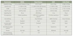
Ultimately, the optimal switching technology depends heavily on the application itself (see the table). A switching architecture optimized for low-level parametric testing may look very different from one designed for high-power automotive semiconductor validation.
Key Design Challenges in High-Channel-Count Switching Systems
Selecting the appropriate switching topology and technology is only one part of designing a scalable semiconductor test system. As channel count increases, engineers must also address several interconnected architectural challenges:
- Maintaining signal integrity as switching matrices grow larger and denser.
- Improving throughput without introducing synchronization issues.
- Managing routing and integration complexity within highly automated test environments.
Addressing these challenges requires careful consideration of switching topology, system architecture, synchronization strategy, and software integration.
Challenge 1: Maintaining Signal Integrity at High Channel Counts
As switching matrices grow larger and denser, maintaining signal integrity becomes more challenging. One of the biggest issues encountered by engineers is parasitic capacitance. As channel count increases, so too does capacitance throughout the switching system, which can negatively affect measurement settling times and overall test speed.
Large switching matrices may also introduce leakage current, insertion loss, crosstalk, and electromagnetic interference. These effects become particularly problematic when measuring low-level analog signals or performing high-precision parametric tests.
To minimize these issues, engineers often divide large switching systems into smaller modular building blocks, rather than create a single massive matrix. Breaking the system into smaller sections can help reduce capacitance, improve isolation, and simplify troubleshooting.
Physical layout plays a major role in signal integrity as well. With growing relay density, magnetic interaction between adjacent relays can affect performance if adequate shielding and isolation aren’t implemented. Similarly, compact system footprints could increase unwanted coupling between signal paths.
Finally, cabling and interconnection strategies must also be carefully considered. The quality of the switching hardware alone can’t guarantee system performance if signal routing throughout the larger test system is poorly managed. As such, engineers must pay close attention to cable routing, grounding, shielding, and separation between sensitive and high-power signal paths.
Challenge 2: Improving Throughput Without Sacrificing Synchronization
While maintaining signal integrity is critical, engineers must also ensure switching architectures support the throughput demands of modern semiconductor production environments. When testing thousands of pins, switching overhead alone can significantly impact overall test time if the switching architecture isn’t optimized for parallel operation.
Topology selection plays a major role here. Multi-bus matrix architectures can enable parallel testing by allowing measurements to occur simultaneously rather than sequentially. This may dramatically improve throughput in high-channel-count systems. However, increasing parallelism also intensifies synchronization complexity. Measurement systems and switching hardware must coordinate closely to ensure measurements aren’t taken while relays are still transitioning between states.
In many systems, instruments and switching hardware communicate using trigger-based handshaking. For example, a source measure unit (SMU) may issue a trigger to the switching system, wait for confirmation that switching has completed and settled, and then initiate the measurement sequence. Without proper synchronization, engineers risk collecting invalid or inconsistent measurement data.
Some switching platforms also incorporate built-in relay-settling management within their software drivers. These capabilities can help simplify synchronization in larger automated test environments.
Challenge 3: Managing Routing and Integration Complexity
As switching architectures scale further, the challenge extends to managing the growing integration, routing, and software complexity associated with larger automated test systems. First, since switching systems often sit in the middle of the test architecture, integration complexity must be well thought out. Semiconductor test systems may combine:
- PXI instrumentation
- LXI rack-mounted hardware
- Programmable logic controllers (PLCs)
- Embedded controllers
- Data-acquisition (DAQ) systems
- Custom software environments
With high-channel-count systems specifically, as previously mentioned, even something as seemingly straightforward as cable management can become a significant system-level challenge. Engineers must carefully route interconnects between instrumentation, switching hardware, and DUT interfaces to minimize interference while maintaining serviceability and scalability.
For the highly complex routing required in these systems, many engineers rely on software-based signal-path management tools that abstract low-level relay operations. Rather than specifying individual relay closures, engineers can define desired signal endpoints, while the software automatically determines the required routing configuration. This approach reduces software complexity, shortens development time, and helps minimize human error.
Similarly, automated diagnostics are also becoming increasingly important in high-channel-count test environments. Features such as relay self-test and system-level diagnostics allow engineers to quickly identify failures and reduce downtime.
Lastly, software compatibility also plays an important role in these large semiconductor test environments. Engineers must ensure that switching platforms support the operating systems, drivers, and control environments already used throughout the test infrastructure. In highly automated environments, even small compatibility or synchronization issues can lead to significant deployment delays and troubleshooting complexity.
The Flexibility of Modular Architectures
Historically, many engineers designing semiconductor test systems have relied on fixed “rack-and-stack” configurations that offer limited flexibility once deployed. This is problematic because expanding these systems often requires a major redesign or complete replacement of the switching infrastructure.
In contrast, modular switching architectures enable systems to scale incrementally as requirements evolve, eliminating the need for frequent large-scale redesigns. This scalability can be especially valuable in semiconductor environments where:
- Production ramps gradually.
- New DUT variants emerge frequently.
- Additional measurements must be incorporated later.
Beyond scalability, modular switching architectures can also help test engineers improve:
- Maintainability and uptime: When switching hardware is modular, failed cards or assemblies can often be replaced quickly, without taking the entire system offline for an extended period.
- Reusability: Engineers are able to reuse existing switching modules, software environments, and instrumentation while adding new functionality as requirements evolve.
- Vendor choice and flexibility: Compared to closed or fully proprietary test systems, engineers maintain greater control over system architecture and can integrate equipment from multiple vendors, rather than rely on a single-source solution.
- Long-term system value: As semiconductor programs evolve, engineers could repurpose switching assemblies and instrumentation across multiple projects or production lines instead of retiring entire test platforms, reducing long-term capital costs.
As semiconductor test requirements continue to evolve, modular switching architectures provide engineers with a more adaptable foundation for balancing scalability, maintainability, and long-term flexibility.
Building Switching Architectures that Scale with Semiconductor Complexity
As semiconductor devices grow in complexity, designing scalable switching architectures requires simultaneously balancing multiple interconnected system-level challenges. As a result, engineers must develop modern high-channel-count semiconductor test systems, while also ensuring switching architectures preserve signal integrity, support throughput requirements, maintain synchronization, and scale alongside evolving test requirements.
This is why modular switching architectures are developing into an essential component within semiconductor test environments. Using a modular approach, engineers can expand systems incrementally, integrate new measurement capabilities, simplify maintenance, and adapt to changing test requirements without completely redesigning the underlying architecture.
>>Download the PDF of this article
 shutterstock_2198551397
About the Author
 Steven Edwards
Steven Edwards
Head of Product Management, Pickering Interfaces
Steven Edwards is head of product management at Pickering Interfaces, where he has spent more than 20 years developing switching and signal-routing solutions for electronic test and verification applications.
Comment About the Article
To join the conversation, and become an exclusive member of Electronic Design, create an account today!
 Leaders Logo
Leaders relevant to this article: