Ring-Oscillator Process Monitors for Wafer-Level CMOS Screening
What you'll learn:
- How a CMOS ring oscillator acts as a sensitive process monitor.
- Where process monitors are placed on a die and why location matters.
- How process monitors fit into the wafer-level test and binning workflow.
- How the transistor technology node affects ring-oscillator design choices.

A process monitor is a dedicated circuit embedded on each die of a wafer, designed to determine which process corner that die belongs to. As the silicon wafer passes through multiple fabrication steps — doping, deposition, and etching — subtle variations accumulate across the wafer, causing each die to behave slightly differently from its neighbors.
These fabrication variations directly impact circuit speed, power consumption, and reliability. By measuring the process monitor's output, engineers can quantify these variations, separate good dies from bad ones, and characterize exactly which PVT corner — Fast-Fast, Slow-Slow, Typical, or a skewed combination — each die belongs.
CMOS Ring Oscillator as a Process Monitor
A ring oscillator is a closed-loop chain of an odd number of CMOS inverters where the output of the last inverter feeds back to the input of the first. Only an odd number of inverters creates the logical contradiction needed to sustain oscillation. Consider a single inverter: it inverts its input (logic 0 -> 1, logic 1 -> 0). Three inverters in a ring invert the signal three times total, so the output is always the complement of what entered, causing the ring to continuously toggle (Fig. 1).

The oscillation frequency depends on two parameters: the per-stage propagation delay and the number of stages:
f_osc = 1 / (2 × N × t_pd)
where N = number of inverter stages and t_pd = per-stage propagation delay.
For a practical process monitor, a 2-input NAND gate replaces the first inverter to provide an Enable control:
Enable = 1: NAND acts as an inverter -> ring oscillates
Enable = 0: NAND output is forced high -> oscillation stops
This allows the automatic test equipment (ATE) to gate the oscillator on for a precise measurement window (Fig. 2).

Sizing in Advanced CMOS Nodes
At 7- and 5-nm FinFET nodes, effective carrier mobility is nearly equal for PMOS and NMOS. Therefore, transistors in the inverter stages can be sized nearly identically:
W_p / W_n ≈ 1.0 to 1.2
This symmetry simplifies balanced ring oscillator design considerably compared to older planar nodes, where PMOS transistors required roughly twice the width of NMOS to achieve equal drive strength.
>>Download the PDF of this article, and check out the TechXchange for similarly themed articles and videos


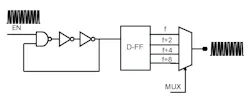
Frequency Division for ATE Compatibility
At advanced nodes, a 3-stage or 7-stage ring oscillator can readily produce oscillation frequencies exceeding 20 GHz, which is well beyond the measurement capability of standard ATE. A chain of D flip-flops divides the output frequency by powers of 2:
f_out = f_osc / 2^n
where n = number of D flip-flop divider stages.
For example, a 32-GHz oscillator divided by 2^6 (= 64) yields approximately 500 MHz, well within standard ATE pin bandwidth. A multiplexer at the divider output lets the test program select the optimal divide ratio for any given oscillator speed (Fig. 3).
Placement on Die and Wafer
Process monitors can be placed in two locations, each with different tradeoffs:
- Active die area: The monitor is embedded within the functional die itself, allowing it to be measured both at wafer sort and during packaged-part testing. This placement reflects actual on-product conditions — same power supply, same temperature gradients — but consumes a small amount of product die area.
- Scribe line: The narrow saw-cut region between adjacent dies on a wafer can also host process monitors. Scribe-line monitors are free in terms of die area, but they’re destroyed when the wafer is diced. They’re measured only during wafer sort, before singulation, and used primarily for process control rather than per-unit binning.
A single die may include multiple process monitors targeting different circuit types; for example, one optimized for NMOS speed, one for PMOS speed, and one for a balanced CMOS path. This allows engineers to detect skewed corners (Fast-NMOS/Slow-PMOS) that might be missed by a single combined monitor.
Applicability Across Transistor Technologies
Ring-oscillator process monitors are used across a wide range of CMOS technology nodes, but their design details vary significantly by generation:
- Planar CMOS (130 to 28 nm): PMOS carrier mobility is roughly half that of NMOS. Thus, PMOS transistors are sized approximately twice as wide (W_p/W_n ~= 2.0-2.5) to achieve balanced rise and fall times in inverter stages.
- FinFET nodes (16 to 5 nm): The fin-based 3D transistor structure equalizes effective carrier mobility between PMOS and NMOS. As a result, sizing ratios converge toward W_p/W_n ~= 1.0-1.2, greatly simplifying balanced oscillator design.
- Gate-all-around (GAA) / Nanosheet (3 nm and below): Emerging nanosheet transistors offer further mobility equalization and additional tuning via nanosheet width. Ring-oscillator design principles remain the same, but layout rules and parasitic extraction become more complex.
In all cases, the ring oscillator targets the same goal: Providing a frequency output that’s a direct, measurable proxy for transistor drive strength and, therefore, process corner.
How Process Monitors Fit into Testing and Verification
Process monitors are measured at two main stages in the production flow:
- Wafer sort (pre-dicing): After fabrication is complete but before the wafer is cut into individual dies, a probe card makes electrical contact with each die in sequence. The ATE enables the ring oscillator, counts output cycles over a fixed time window, computes frequency, and compares it against binning limits. This step catches gross process outliers before the cost of packaging is incurred.
- Final test (post-packaging): For monitors embedded in the active die area, the measurement can be repeated on packaged parts. This allows engineers to correlate any frequency shift between wafer sort and final test, which can reveal packaging-induced stress or thermal effects.
During early process development and characterization, engineers measure process monitors across many wafers and lots to build a statistical model of the process distribution. These measurements define the Fast-Fast, Slow-Slow, and Typical corner boundaries. In production, each die's measured frequency is compared against these pre-characterized limits to assign it to a performance bin.
Dies whose frequency falls outside the acceptable range are ink-marked (or flagged in the ATE data file) and excluded from packaging. High-frequency dies may be binned into premium speed grades; low-frequency dies may be downgraded or scrapped, depending on the product family.
Conclusion
When a process monitor is measured on-die, its output frequency provides direct PVT (Process, Voltage, Temperature) information. For a monitor with a nominal frequency of 10 to 12 GHz:
- A measured frequency above 13 GHz indicates the FF (Fast-Fast) corner — fast transistors with potential leakage current concerns.
- A measured frequency below 9 GHz indicates the SS (Slow-Slow) corner — slow transistors where timing closure becomes a concern.
The process monitor is an elegant, low-cost, minimal-area solution for measuring process variation across a wafer. It exploits the well-defined relationship between ring-oscillator frequency and transistor performance to enable fast, reliable binning at production scale.
>>Download the PDF of this article, and check out the TechXchange for similarly themed articles and videos
About the Author

Preethi Ashwath
Senior Analog Design Engineer, Analog Devices Inc.
Preethi Ashwath is a Senior Analog Design Engineer at Analog Devices Inc., based in the Boston area, where she works on mixed-signal IC design for the consumer electronics domain. She holds an M.S. in Electrical Engineering from the University of California, Irvine, and graduated with multiple gold medals from Visvesvaraya Technological University.
Preethi also serves as a reviewer for IEEE flagship conferences such as ISCAS and MWSCAS, and was selected as a technical presenter for Analog Devices at CES 2025.
Comment About the Article
To join the conversation, and become an exclusive member of Electronic Design, create an account today!

Leaders relevant to this article: