A SiP of Reliable Advantage—Systems Under Test

>> Electronic Design Resources
.. >> Library: Article Series
.. .. >> Series: Path to Systems
In parts 1, 2, and 3 of the series, we talked about how the fundamental shift of focus toward systems makes system-in-package (SiP) an essential step forward in electronic design. Through SiP, a complete system can be packaged into a standard ball-grid-array (BGA) package the size of a nickel, such as the Octavo Systems’ OSD335x in Figure 1.
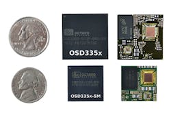
1. The OSD335x is an example of a complete system fitting into a tiny BGA package.
We also discussed the advantages SiP brings to the design and manufacturing of semiconductors and how they can be used to tip the economy of scale toward low-volume opportunities. In this article, we will examine testing methodologies for SiP and how it simplifies testing and characterization of devices. This gives customers of SiP a more-reliable, higher-quality product to put into an end system.
There are several advantages to manufacturing a product or device using a system component (i.e., a SiP) rather than using discrete components. Here, we will focus on the advantages found in the device testing process and methodology. SiP components are uniquely suited to take advantage of the semiconductor manufacturing processes while simultaneously utilizing system-level testing normally reserved for the end product or device.
While Moore’s Law has driven ever-increasing transistor densities and device complexity, semiconductor testing has kept pace by focusing on extremely high-volume manufacturing. This necessitates moving quickly through the manufacturing learning curve to reduce the cost of a product as quickly as possible. As a result, the semiconductor test methodology and equipment used during manufacturing have not only made semiconductor component testing extremely cost-effective, but have also resulted in higher quality and more reliable devices.1
With this as a backdrop, let’s first explore some basic testing concepts of both semiconductor devices and systems. That follows with a look at a SiP as a device under test (DUT) and application of these concepts.
Testing Basics
Generally, the further down the manufacturing process an unusable device travels, the more money is lost. It’s therefore important to test as much as possible early in the manufacturing process. In addition, as devices become more differentiated, they become more expensive to test as the volume of the devices drops and the process becomes more manual.
For example, the component tests for a generic CPU are much more automated than system-level tests on specialized equipment using that CPU. As such, each subsequent round of testing should focus on aspects that weren’t tested or couldn’t be tested earlier in the process. This applies to both component-level testing of semiconductor devices as well as system-level testing required for products or devices.
Traditionally, semiconductor testing is focused on components rather than systems since most semiconductor devices are used as discrete components within a larger system. Component testing is primarily divided into two parts: wafer-level testing and packaged-device testing.
In a wafer probe,2 the equipment will initiate different tests by probing each die in order to determine good die that will be packaged for further testing. Once the semiconductor die is packaged, the test equipment can perform the next set of tests, which includes external circuits, in order to finalize the component to be sold.
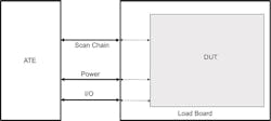
Due to the volume of products manufactured in the semiconductor world, the component-level testing uses automated test equipment (ATE) (Fig. 2). Such ATEs use input vectors, patterns of 1s and 0s, or voltages designed to test for and uncover faults in the DUT. This is done by comparing the actual output vectors of the DUT to the expectations of the design specification, datasheet, and/or statistical characterization of known-good devices. ATEs are designed to use different test fixtures depending on the testing process and device to provide high test throughput and minimize the idle time of the ATE. For example, load boards enable automatic handling of packaged devices.

2. A typical automated test equipment (ATE) setup. (Courtesy of Advanced Semiconductor Engineering Inc.)
Figure 3 shows a simple block diagram of an ATE interacting with a packaged DUT via a load board and a flow graph of how it tests the DUT. While the ATE can have access to some or all of the pins of a given device, the primary interaction between the ATE and complex DUTs, such as a processor or system-on-chip (SoC), is generally via a JTAG (Joint Test Action Group) Test Access Port (TAP) and boundary-scan chain infrastructure (Fig. 3, top). These elements inside a DUT can be accessed via a JTAG interface, which allows the testing of a device with different methodologies, such as automatic test pattern generation (ATPG) to detect stuck-at faults, built-in self-test (BIST) to detect faults in both memory and logic,3 or functional tests like IO loopback (Fig. 3, bottom).

3. ATE test setup with load board and DUT (top); flow graph of how the ATE tests the DUT (bottom).
Traditionally, when building real-world products or devices, a system-level testing (SLT) methodology4 is used. Generally, this involves loading production software or firmware on to the system and testing the system-level functionality of each component by covering all of the intended use cases. In many cases, this process is more manual.
An interesting example comes from the early part of Gene Frantz’s career on the manufacturing production line in the Texas Instruments calculator division. Instead of an ATE, many times the production tester was a human. The production test on the DUT (in this case, a calculator) consisted of a set of test vectors (an equation) entered into the DUT and the output test vector (resulting answer to the equation) being read by the tester (human) with a determination of pass or fail. Depending on the volume of production, this type of manual testing process is still used today for system-level testing.
System-in-package devices, on the other hand, fall somewhere in between. They incorporate many tested die themselves, as well as other semiconductor components connected together. As such, they can be considered a system, requiring system-level testing. However, the good die may not have been as fully tested as individual packaged devices and, therefore, can’t be considered a component, requiring component-level testing in SiP. This leads to the question: How should a SiP be tested?
How Should the SiP be Tested?
System-in-package devices can consist of multiple active and passive components. To test every component individually, all of the pins of each component need to be brought out to a pin/ball on the SiP. While this would enable full component-level packaged-device testing, it also drastically reduces the benefits of a SiP. Since manufacturing testing shouldn’t reduce the design, cost, and size benefits of a SiP, a hybrid approach is required to verify and validate a SiP.
Component-level testing should be employed for all direct connections between die and the package pins/balls. This will ensure that there are no structural faults and provide a platform for characterization similar to what would be performed on standard packaged components.
On the other hand, system-level testing should be employed to validate and characterize all internal connections. This could include functional-level tests to validate connections between components, such as a processor and DDR memory. It could also involve stress tests to verify proper operation under heavy loads, e.g., confirming that a power-management IC (PMIC) can supply enough current to meet system needs. SiP devices may also use some pins/balls as test points (i.e., pins that should not be used functionally) to provide visibility on internal signals. For example, test points can be employed to monitor voltage rails only used within the SiP.
Using a hybrid testing approach for SiP devices provides several benefits. First, since components are already connected together within the SiP, those intermediate connections no longer have to be tested as rigorously as they would when testing the component individually. For example, if a PMIC provides a voltage rail that’s used completely within the SiP, the PMIC output no longer must be fully characterized for all potential output loads since the output load is, by design, fixed.
Similarly, the input pins of all components attached to that voltage rail no longer need to be tested over a wide range of input voltages since that, too, is fixed. This allows for a reduction in the component-level tests required, since that connection can now be validated by a single system-level test. In addition, the form factor of a SiP makes it possible to utilize semiconductor ATEs, which can reduce the time needed for handling during many system-level tests and automate what might have otherwise been a manual process.
Testing a SiP as a Semiconductor
Given the SiP form factor, it can be handled as if it were a semiconductor component. Socketed load boards (i.e., load boards that allow an ATE to connect to one or more DUTs) enable the ATE to send test vectors to the DUT and verify the resulting vectors of the test. In addition to validating the test vectors, the ATE can also perform open and short testing as well as voltage-level verification on the DUT. For example, the following diagrams describe how the OSD3358 SiP from Octavo Systems is tested as a semiconductor component rather than as a typical end system, such as a printed circuit board (PCB) or system-on-module (SoM).


4. ATE setup to test a SiP (top); flow graph of the ATE testing the SiP (bottom).
As shown in Figure 4 (top), the ATE interfaces with the SiP and non-volatile memory on the load board. The socketed load board provides the ATE with access to all of the SiP device’s pins. Figure 4 (bottom) shows the flow graph of the test procedure. Open and short testing is first performed to eliminate DUTs (in this case, SiPs) with manufacturing faults that resulted in unconnected or shorted signals. The ATE then supplies power and verifies the voltage levels of the SiP. Finally, a software program contained in the non-volatile memory, which includes functional tests, is copied into the SiP during boot and is used to examine the rest of the SiP. This program interfaces to the ATE through the test vector input and output interface whereby the ATE can then send the commands to control which tests are executed by the SiP. Figure 5 shows the OSD335x SiP undergoing test.

5. The OSD335x-SM SiP under test. (Courtesy of Advanced Semiconductor Engineering Inc.)
These tests might include verifying the hardware inside the SiP or validating various interfaces. After each test, the SiP can send an output via the vector interface that reflects the outcome of the test. Consequently, that part can be sorted and binned based on whether the device passed or failed the test. In general, the tests should be as short as possible and ordered based on which covers the most common failures, so that “bad” devices can be found as quickly as possible.
There are several advantages to this methodology. It’s easy to update the non-volatile memory to add more tests or update existing tests. In addition, the quick feedback loop between the DUT and the ATE means that failures are identified faster and in a completely automated manner. Boot time is minimized since the DUT need only boot and load the tests one time. This can result in shorter test times, which reduces the cost of the device.
Yield
While many testing benefits can be realized with SiP technology, one classical concern often raised is yield. The argument is, given that SiP can contain hundreds of components, each with their own failure rate, the final yield of a SiP is the product of the yields of individual components. For example, if you have five components within a SiP, each with a 95% yield, theoretically the resulting SiP yield is only approximately 77% (0.95 * 0.95 * 0.95 * 0.95 * 0.95 ≈ 0.77). However, this isn’t what’s actually seen.
In reality, SiP yields are much higher due to a combination of factors. As discussed above, when discrete components are tested, all inputs and outputs must be fully tested. Furthermore, tighter test limits, or guard-banding, are applied to ensure that the component can be used in all extremes of the use conditions called out in the general-purpose specifications.
But, within a SIP, the use environment is known and controlled. For internal connections, variation in input voltage, current load, timing, and other variables are minimal. Therefore, devices that might have otherwise failed the normal component testing can be used within a SiP because it meets the requirements for the given SiP. Hence, SiP yields depend on the system use requirements, more like an end product, rather than just the individual component yields.
As more semiconductor companies look to make their devices “SiP ready,” refinements in device testing will occur in wafer-level testing, enabling further improvements in SiP yields. Eventually, wafer-level tests will include any provision to make physical changes in chips, such as resistor trimming or fuse blowing, as well as additional test coverage to avoid complex testing in SiP form.
Conclusion
By using a hybrid of component- and system-level testing methodology, SiP offers benefits to the system manufacturer as well as the end customer of a more robust and cost-effective product. This is achievable if SiP manufacturers perform system tests while utilizing the testing methodologies and infrastructure of semiconductor testing.
We have found this method to yield extremely high rates of pass at next-level system tests. This unique method of testing, in addition to all of the other benefits of using a SiP device discussed in this series, provides strong arguments that a SiP solution like that developed by Octavo Systems may be the best solution for any embedded product design.
- Series: Path to Systems
- Prior article in this Series ... SiP—Leveraging Mass Production on a Small Scale
- Next article in this Series ... The Time of System-in-Package Has Arrived
- https://www.electronics-notes.com/articles/test-methods/automatic-automated-test-ate/basics-primer.php
- https://anysilicon.com/ultimate-guide-wafer-sort/
- https://www.electronicdesign.com/test-amp-measurement/what-s-difference-between-atpg-and-logic-bist
- https://semiengineering.com/toward-system-level-test/

About the Author
Neeraj Dantu
Applications and Systems Engineer
Neeraj Dantu is an Applications and Systems Engineer at Octavo Systems. As a recent graduate, Neeraj is excited to be a part of Octavo’s highly experienced team. He also looks forward to help Octavo change the face of electronic design and manufacturing. With diverse research experience in hardware design, machine learning, computer vision, and signal processing, Neeraj brings a fresh perspective to the team. Neeraj earned his B.Tech (Bachelor of Technology) in Electronics and Communications Engineering from The LNM Institute of Information Technology, India, and a Masters in Electrical Engineering from Rice University.
Gene Frantz
Chief Technology Officer
Masood Murtuza
Co-founder and Manager of Package Engineering
Masood Murtuza is the Manager of Package Engineering and a founder of Octavo Systems. Prior to joining Octavo, Masood was a Fellow at Texas Instruments, where he held various leadership roles in the Packaging and Assembly Process Engineering teams. During his tenure at TI, he introduced a number of new semiconductor packaging technologies. He also helped advance innovation in technology development across the company by establishing new methodologies in package and assembly development process. Masood holds 25 patents and has authored or co-authored over 15 papers. He received his BTech in Mechanical Engineering from the Indian Institute of Technology, Madras, India, and an MSc in Naval Architecture from University College, University of London.
Erik Welsh
Applications and Systems Manager
Erik Welsh is the Applications and Systems Manager for Octavo Systems. Erik comes to Octavo after spending three years as the Principal Systems Architect at Mango Communications developing platforms for cutting-edge wireless research targeting the WARP (Wireless Open-Access Research Platform) project. Prior to that, he spent 11 years at Texas instruments in a variety of engineering and customer support roles.
He began his career as a system-on-chip (SoC) designer eventually leading SoC Security Architecture development. He later spent time as an Applications Engineer supporting industry-leading customers in the PC industry. Erik earned a Bachelor of Science and Masters in Electrical Engineering from Rice University.
Gene Frantz
Chief Technology Officer
Gene Frantz is one of the founders and the visionary behind Octavo Systems. He currently serves as Chief Technology Officer. He is also a Professor in the Practice at Rice University in the Electrical and Computer Engineering Department. Previously, Gene was the Principal Technology Fellow at Texas Instruments, where he built a career finding new opportunities and building new businesses to leverage TI’s DSP technology. Through this work he became highly regarded in the industry as a leader in DSP technology. Gene holds 48 patents, has written over 100 papers/articles, and presents at conferences around the globe. He has a BSEE from the University of Central Florida, a MSEE from Southern Methodist University, and a MBA from Texas Tech University. He is also a Fellow of the IEEE.
Comment About the Article
To join the conversation, and become an exclusive member of Electronic Design, create an account today!

Leaders relevant to this article: