Why Traditional VVC Will Outlive the Neural-Codec Hype on Silicon
What you’ll learn
- Why an end-to-end neural video decoder costs roughly an order of magnitude more energy per pixel than mature VVC silicon at the same process node.
- Where the hybrid path - JVET’s NNVC neural tools on a VVC core - is worth the area, power, and verification cost, and where its 10–12% BD-rate gain does not pay back the silicon.
- How a tier-aware deployment strategy that keeps a traditional VVC (or AV1) decoder as the primary path while adding neural tools only when standards and budget allow.

There is a lot of excitement on neural networks, artificial intelligence and machine learning in 2026, and naturally their implementation on video codecs has been on the radar. Some research suggests end-to-end learned codecs match or beat Versatile Video Coding (VVC) under specific test conditions.
Joint Video Experts Team (JVET) is running formal exploration experiments on neural tools for a potential future standard. However, the question is whether any of these should change near-term SoC roadmaps.
Looking at the actual hardware budgets, the conclusion is that traditional VVC will not be displaced from consumer silicon in the next decade. Neural-based video coding may be winning on the algorithmic end but losing on the silicon floor. Hardware costs for end-to-end neural decoders are roughly an order of magnitude worse on energy per pixel than mature VVC silicon at the same node, and standardization for fully neural codecs does not exist. The hybrid path, JVET’s Neural Network-based Video Coding (NNVC) intra prediction added to a VVC core, has lower but still meaningful hardware cost. It is viable in premium-tier consumer ASICs only if a future standard ratifies it (Fig. 1).
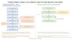
Why neural codecs are being explored
Each generation, from H.264 to HEVC to VVC, has delivered roughly 30-50% bit-rate reduction over its predecessor, but sustaining that trajectory is getting expensive. In all-intra encoding, the VVC reference encoder is already about 31× more complex than HEVC’s, measured as reference-software runtime (VTM vs HM), and the driver is the growing number of prediction modes each generation: for example, angular intra modes alone went from 8 in H.264 to 33 in HEVC to 65 in VVC. However, creating and exploring human hand-crafted coding tools for a significant improvement on the compression is getting tougher with each generation.
Neural video coding has arrived in this context, and its appeal is that learned tools can capture compression and perceptual quality that hand-designed algorithms cannot, with gains coming from training and data rather than another decade of hand-crafted coding tools. JVET’s NNVC exploration has adopted two neural tools into its reference software, though not yet into a normative standard: a fully connected intra prediction mode and a convolutional in-loop filter, with combined Y BD-rate gains around 10-12% across configurations.
The NN intra prediction mode is signaled per block via an nnFlag and competes with the existing 67 intra modes, MIP, ISP, MRL, and CCLM through rate-distortion optimization rather than replacing them. End-to-end neural codecs (DCVC-FM, NVRC) match or exceed VVC under specific test configurations such as single-I-frame or random-access on UVG; NVRC outperforms VVC by 24% BD-rate on UVG, and DCVC-family codecs produce subjectively smoother low-bitrate images than VVC under several quality metrics. The problem comes when these results must fit in consumer devices like a phone (thermal/power budget and multi-tasking with other AI workloads), TV (standardization challenges, cost sensitivity, energy star ratings), or automotive infotainment (functional safety verification cost and NPU contention with other safety-critical operations).
What the silicon actually costs
Traditional VVC hardware decoders are extraordinarily efficient. Production IP cores deliver up to 8K decoding. The closest published anchor for full-decoder energy efficiency is the Tikekar et al. HEVC decoder ASIC at TSMC 40 nm, measured at 1.19 nJ per pixel for 4K30. Scaling forward by the historical 30-50% per-node power reduction from 40nm to 28nm and applying the roughly 1.6-1.8× HEVC-to-VVC complexity uplift, a 4K60 VVC decoder at 28 nm plausibly lands around 1-1.5 nJ/pixel within about 1 million gates. Production VVC IP figures are proprietary and not directly published.
The only published end-to-end neural decoder ASIC, NVCA, is the cleanest data point. Synthesized in TSMC 28 nm with 5.01 million gates (excluding weight ROMs that are stored off-chip), it achieves 1080p25 at 760 mW, which works out to roughly 14.6 nJ per pixel. The power and area numbers are orders of magnitude more than traditional VVC at the same node.
The hybrid path (JVET’s NNVC experiment) has fewer hardware challenges than NVCA, but it is also not free. NNVC neural intra prediction specifies 7 fully-connected networks (one per supported block shape from 4×4 to 16×16) of roughly 1216 neurons per layer, invoked on perhaps 30-40% of intra blocks. If the standard ratifies NNVC, the practical hardware path is a single shared MAC array that time-multiplexes the 7 block-shape-specific weight sets, loading the appropriate set into the array at the start of each block-level inference and holding it stationary during compute.
Weights would live in on-chip ROM, analogous to VVC’s MIP and LFNST coefficients. NNVC intra prediction adds compute load to the VVC decoder pipeline under tight latency cycle budgets, since NN-based decoding takes substantially more cycles than traditional algorithms to generate an output. The added area, power, and verification cost are non-trivial. They are defensible on premium SoCs once the tool is standardized, but hard to justify on cost-sensitive parts where the 10-12% BD-rate gain doesn’t pay back the silicon.
Standardization is also a deciding factor. The final NNVC decoder’s bit-exact fixed-point inference must match across devices. This is a constraint that forecloses many standard NPU efficiency techniques such as reduced-precision inference and fused operators. VVC is finalized as ITU-T H.266 with established licensing. NNVC is still in JVET’s exploration phase. End-to-end neural codecs are further back yet, with no ratified standard, no cross-vendor interoperability, and no royalty framework to build a product around. This is a problem for consumer hardware, where compliance is mandatory.
The solution: tier-aware deployment, not wholesale replacement
Keep traditional VVC as the primary path. The VVC (or AV1) decoder block is the right choice for the next five to seven years. It is mature, deterministic, and supported across the full range of relevant nodes, and VVC content will be decoded for two decades after the standard’s 2020 finalization. Skipping it for neural codecs is misguided.
Add NNVC tools as auxiliary blocks when standardization and budget allow. Couple a small NN inference block to the VVC decoder, plan ROM for the normative weight sets and SRAM for working storage, match SADL bit-exactly, and budget for non-trivial verification.
A general-purpose end-to-end neural decoder block does not belong in consumer SoCs for the next few SoC generations. Hardware cost is too high, standardization does not exist, and the ecosystem does not justify it. End-to-end neural codecs may have limited use in specialty scenarios such as VR/AR, machine vision, and edge encoding co-designed with the hardware.
What it means for a tape-out
For chip architects, the guidance is concrete. Do not skip VVC hardware support to chase neural codecs, and do not over-provision NPU capacity for adoption that will not arrive on schedule. Plan tier-aware deployment, tie any neural tool adoption to standardization timelines, and let the tape-out reflect the world that exists. The more conservative silicon is the right call here. The dramatic replacement narrative, even if it is ultimately feasible, will take decades to materialize.
About the Author
 Dhruv Aggarwal
Senior RTL Design Engineer
Dhruv Aggarwal is a Senior RTL Design Engineer at NVIDIA Inc in Santa Clara, California, working on the micro-architecture of display and GPU hardware, including low-power design of pixel-processing pipelines. He previously spent five years designing area-optimized spatial-prediction hardware for the HEVC, AV1, and micro-architecting H.266/VVC video codecs at Qualcomm. He is a co-inventor on patents covering chroma-from-luma prediction (US 12,395,655) and reference-pixel upsampling for intra-prediction in video coding (US 11,595,665), and holds an MS in Electrical Engineering from Columbia University. The views expressed in this article are his own and do not represent any employer.


Comment About the Article
To join the conversation, and become an exclusive member of Electronic Design, create an account today!
 Leaders Logo
Leaders relevant to this article: