Driving Innovation in 3D IC: Chiplet Summit
What you’ll learn:
- Why we need chiplets to address issues like the reticle limit.
- What design considerations are there for 3D IC packaging?
- How do issues like thermal design differ with 3D IC packages?
3D IC solutions based on chiplets provide many advantages, such as enabling designs that exceed the reticle limit for a monolithic die. Kevin Rinebold, Technology Manager 3D IC Solutions at Siemens EDA, presents issues and solutions for designers of 3D ICs (watch the video above).
Transistors are shrinking, but the number of transistors in a die is growing — especially for high-performance processors, GPUs, and neural processing units (NPUs). Also, the gap is widening between compute and memory speeds (Fig. 1).
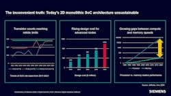
The difference in silicon technologies used for compute and memory speeds is changing how solutions are designed. High-bandwidth-memory (HBM) chiplets allow wide, fast RAM to be interfaced with compute die that use smaller transistors. This mix would not work on a monolithic die.
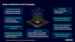
Moving to a chiplet-based, 3D IC packaged system provides a number of benefits, but more design considerations come into play for a system that’s already very complex (Fig. 2). Details like connectivity have led to the development of interfaces such as the UCIe Consortium’s Universal Chiplet Interconnect Express (UCIe).
3D ICs make it possible to build advanced artificial-intelligence (AI) chips. However, designing, testing, and delivering them requires EDA and product lifecycle tools like those available from Siemens EDA. They take advantage of advanced, multi-physics modeling as well as standards like UCIe.
More Coverage of the 2026 Chiplet Summit

About the Author

William G. Wong
Senior Content Director - Electronic Design and Microwaves & RF
I am Editor of Electronic Design focusing on embedded, software, and systems. As Senior Content Director, I also manage Microwaves & RF and I work with a great team of editors to provide engineers, programmers, developers and technical managers with interesting and useful articles and videos on a regular basis. Check out our free newsletters to see the latest content.
You can send press releases for new products for possible coverage on the website. I am also interested in receiving contributed articles for publishing on our website. Use our template and send to me along with a signed release form.
Check out my blog, AltEmbedded on Electronic Design, as well as his latest articles on this site that are listed below.
You can visit my social media via these links:
- AltEmbedded on Electronic Design
- Bill Wong on Facebook
- @AltEmbedded on Twitter
- Bill Wong on LinkedIn
I earned a Bachelor of Electrical Engineering at the Georgia Institute of Technology and a Masters in Computer Science from Rutgers University. I still do a bit of programming using everything from C and C++ to Rust and Ada/SPARK. I do a bit of PHP programming for Drupal websites. I have posted a few Drupal modules.
I still get a hand on software and electronic hardware. Some of this can be found on our Kit Close-Up video series. You can also see me on many of our TechXchange Talk videos. I am interested in a range of projects from robotics to artificial intelligence.