HBM4 and SPHBM4: Scaling Memory Bandwidth for AI and HPC
What you'll learn:
- Why AI and HPC compute scaling is outpacing DRAM and interconnect bandwidth — and what that means for system utilization and power.
- How HBM4/HBM4e increase I/O count, data rates, and stack heights to raise both bandwidth and capacity versus HBM3.
- How SPHBM4 targets HBM-class throughput on organic substrates and can enable more memory stacks per die edge for new cost/performance tradeoffs.

Over the past two decades, the raw compute capability of processors used in high-performance computing (HPC) and artificial-intelligence (AI) systems has increased at an extraordinary pace. Figure 1 illustrates this trend: XPU floating-point performance has scaled by more than 90,000X, while DRAM bandwidth and interconnect bandwidth improved by only about 30X over the same period.
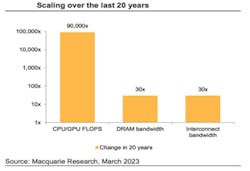
This growing disparity between compute capability and data movement — often described as the memory wall and the I/O wall — has become one of the most significant constraints on achievable system performance.
For system designers, that imbalance translates directly into underutilized compute resources, rising power consumption, and increasing architectural complexity. As a result, memory bandwidth and packaging technologies have become just as critical to AI performance scaling as transistor density or core count.
HBM as a Foundation for Modern AI Architectures
To address these bandwidth challenges, HPC and AI systems have increasingly adopted disaggregated architectures built around chiplets. While LPDDR and DDR memories continue to play important roles, high bandwidth memory (HBM) has emerged as the highest-bandwidth DRAM solution available and a key enabler for modern accelerators.
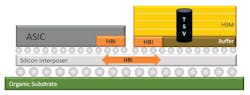
HBM devices consist of a buffer (or base) die at the bottom and multiple 3D-stacked DRAM layers above it. The buffer die uses very-fine-pitch micro-bumps, allowing the memory stack to be co-packaged with an ASIC using advanced packaging technologies like silicon interposers or silicon bridges.
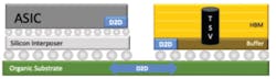
Supported by rigorous standardization through the JEDEC HBM task group, HBM has become one of the most successful and widely adopted examples of chiplet-based integration in production systems. Figure 2 shows a representative side view of an HBM DRAM stack connected to an ASIC through a silicon interposer.
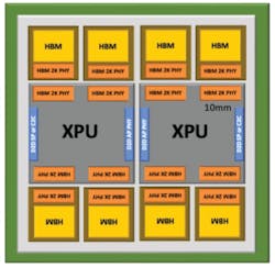
A widely deployed example of HBM in practice is NVIDIA’s B100 Blackwell accelerator (Fig. 3). The package contains two large, reticle-sized XPU dies connected to one another through high-bandwidth links, with HBM devices placed along the top and bottom edges of each die. Each XPU die integrates four HBM stacks — two on each long edge — resulting in a total of eight HBM devices per package.
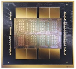
Using typical HBM3 specifications available at the time the JEDEC standard was adopted, each HBM3 device could employ an 8-high stack of 16-Gb DRAM layers, providing 16 GB of capacity per stack. With a data rate of 6.4 Gb/s and 1,024 I/Os, each HBM3 device delivers approximately 0.8 TB/s of bandwidth. Across eight devices, this configuration offers 128 GB of total memory capacity and roughly 6.6 TB/s of aggregate bandwidth.
HBM4: Scaling Bandwidth and Capacity
To continue scaling memory performance alongside compute, JEDEC recently published JESD270-4, the HBM4 standard. HBM4 introduces a number of architectural improvements over HBM3 that directly address the growing bandwidth and capacity requirements of AI workloads.
>>Check out more of our 2026 Chiplet Summit coverage, as well as similary themed articles in these TechXchanges


One of the most significant changes in HBM4 is a doubling of the channel count, increasing the number of I/Os from 1,024 to 2,048. In parallel, supported data rates have climbed into the 6- to 8-Gb/s range and beyond. Memory density has also scaled, with 24- and 32-Gb DRAM layers specified, along with support for 12- and 16-high stacks. Reliability, availability, and serviceability (RAS) features, including DRFM, have also been enhanced.
Taken together, these advances enable substantial improvements in bandwidth, power efficiency, and capacity relative to HBM3. As an example, an HBM4e device using a 16-high stack of 32-Gb layers provides 64 GB of capacity per device (Fig. 4).
With 2,048 I/Os operating at 8 Gb/s, such a device can deliver up to 2 TB/s of bandwidth. In a package containing eight HBM4 devices, total memory capacity scales to 512 GB — 4X that of the earlier HBM3 example — while aggregate bandwidth exceeds 16 TB/s, a 2.5X increase.
Custom HBM and the Role of the Base Die
As HBM4 adoption accelerates, some system designers are exploring the development of custom HBM solutions optimized for specific applications. A key enabler of this trend is the evolution of the HBM base die.
In earlier HBM generations, the base die was typically manufactured using a DRAM-optimized process, well-suited for capacitor structures but less optimal for high-speed logic. With HBM4, most suppliers are transitioning to standard advanced logic processes for the base die. This shift aligns more closely with the processes already familiar to SoC designers and opens the door to customization opportunities.
Whether using standard or custom HBM4 devices, these solutions continue to rely on advanced packaging and silicon substrates, such as interposers or bridges, to accommodate the large number of fine-pitch connections between the memory and the ASIC.
SPHBM4: Bringing HBM‑Class Bandwidth to Organic Packaging
Despite its performance advantages, traditional HBM integration requires advanced packaging, which can drive up cost and complexity. Many system designers, particularly those focused on volume production and reliability, prefer standard organic substrates. To address this gap, JEDEC announced that it’s nearing completion of a new standard for Standard Package High Bandwidth Memory (SPHBM4).
SPHBM4 devices use the same DRAM core dies as HBM4 and provide equivalent aggregate bandwidth, but they introduce a new interface base die designed for attachment to standard organic substrates. Figure 5 illustrates a side view of an SPHBM4 DRAM mounted directly on an organic package substrate, alongside an ASIC. The ASIC itself may also reside on the organic substrate, or it could remain on advanced packaging such as a silicon bridge for multi-XPU integration.
To achieve HBM4-class throughput with fewer pins, SPHBM4 employs higher interface frequencies and serialization. While HBM4 defines 2,048 data signals, SPHBM4 is expected to use 512 data signals with 4:1 serialization, enabling the relaxed bump pitch required for organic substrates.
Because SPHBM4 uses the same DRAM stacks as HBM4, per-stack capacity remains unchanged. However, organic substrate routing supports longer channel lengths between the SoC and memory, which can enable new system-level tradeoffs. In particular, longer routing distances and angled trace routing often allows for more memory stacks to be placed around a given die.
Figure 6 illustrates this effect. When HBM devices are mounted on silicon substrates, they must be placed immediately adjacent to the XPU, limiting the number of stacks to two per 25-mm die edge. With SPHBM4 on an organic substrate, three memory devices can be connected along the same edge, increasing both memory capacity and bandwidth by approximately 50%.
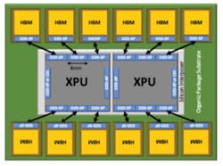
Even when a silicon substrate is still used beneath the XPU — for example, to support high-bandwidth XPU-to-XPU links — the overall interposer size can be significantly reduced when memory devices are moved to the organic package. This reduction could translate into meaningful benefits in system cost, manufacturability, and test complexity.
Looking Ahead
AI workloads continue to push the limits of memory bandwidth, capacity, and packaging technology. JEDEC’s HBM4 standard represents a major step forward in addressing these demands. And the emerging SPHBM4 standard expands the design space by enabling HBM-class performance on standard organic substrates.
For system architects, these technologies offer new flexibility in balancing performance, cost, and integration complexity. As memory and packaging increasingly shape overall system capability, early consideration of options such as HBM4, custom HBM, and SPHBM4 will be essential to fully unlocking the next generation of AI and HPC performance.
>>Check out more of our 2026 Chiplet Summit coverage, as well as similary themed articles in these TechXchanges
About the Author
Kevin Donnelly
Vice President, Strategic Marketing, Eliyan
Kevin Donnelly is Vice President of Strategic Marketing at Eliyan.
Comment About the Article
To join the conversation, and become an exclusive member of Electronic Design, create an account today!

Leaders relevant to this article: