Rethinking AI Architecture: How FPGAs Enable Intelligence at the Edge
What you’ll learn:
- How FPGAs help with AI edge applications.
- FPGA advantages when it comes to AI support.

The accelerating pace of artificial-intelligence (AI) development is massively ramping up its adoption across a broad swath of applications. AI is finding its way into everything from smart personal assistants and image creation to autonomous vehicles.
The ability of AI to make sense of large amounts of data, identify patterns, create insight ,and recommend actions is becoming commonplace. That ability, however, depends on access to a stream of source data and large amounts of compute capability to perform the inference.
Compute requirements are outpacing traditional sequential approaches while time-to-market and solution agility require flexibility in design approaches and adaptability of the underlying hardware platform. In turn, the next generation of ultra-efficient FPGAs is increasingly being embraced to deliver a flexible design environment that blurs the lines between software design approaches, highly parallel compute acceleration, and custom system optimization. The result is rapid development cycles in a power- and compute-efficient platform capable of migrating AI toward the network edge.
The Case for AI at the Edge
If the raw material of AI is data, then it makes sense that the AI capability should be as close as possible to the location of that data. In that way, rapid analysis can be achieved while the data still has context and can be actioned.
Sensor data from an autonomous vehicle demands immediate action while data from an end-of-line quality inspection in high-speed automated manufacturing rapidly loses context after the product leaves the inspection station. Modern systems from medical analysis to robotics produce vast quantities of data from a wide diversity of sensors.
If this data is to be analyzed in a timely manner, then the AI capability needs to be located next to where the data is created, at the far edge of the network where the format of the diverse data streams and the time-critical nature of their content have immediate context. Processing data at the edge also avoids costly and energy inefficient data movement to and from a data center, while helping to preserve confidentiality by not moving sensitive data across public networks.
This doesn’t mean that all AI needs to be dispersed to the network edge. In many applications, AI needs access to a broad diversity of information from across the network or indeed the internet. In these cases, and cases where AI needs access to vast compute capabilities — e.g., in the training of models — then access to the resources of a data center may well outweigh the advantages of a distributed architecture.
For most cases, though, and particularly for inference, a distributed AI capability is highly desirable for rapid, low-latency analysis, for preservation of privacy of data, to avoid costly and time-consuming movement of large quantities of data, and to perform analysis in the same location where the data resides and still has local meaning.
The edge of the network is a very different place from the climate-controlled, resource-rich environment of the data center. At the edge, power and space are very often constrained. Highly reliable operation is needed to avoid costly truck rolls and devices must be secure by design since they reside in an unsecured environment that exposes a large attack surface.
Edge AI systems, therefore, are designed for low-power operation while retaining the compute capability required by the underlying AI model. They’re required to have a small physical footprint to fit into space-contained applications. They must have the ability to monitor their own operation and recover to a functional operating state if anomalies are found. And they have to be secure and cost-effective enough to be deployed at high volume across the network edge.
Technology Alternatives for Edge AI
From the very early days of digital electronics, conventional design approaches have defined some form or arithmetic logic unit (ALU) and register structures to feed input data and store the result. While microprocessors and microcontrollers have increased in complexity and diversity, the underlying premise is to use development tools to adapt an algorithm to “run” on an immutable processing core.
Custom software running on standard processor architectures has delivered fast time-to-market on cost-effective hardware platforms, resulting in added functionality in everything from the personal computer to the domestic refrigerator. However, traditional CPU architectures running software do so in an essentially sequential flow where software executes on the underlying hardware one instruction at a time. This is diametrically opposite to the massively parallel architectural requirements of AI and will fall short of the performance required.
If the general-purpose silicon architecture of the CPU/software solution can’t deliver the required performance, then a logical alternative is to create custom silicon solutions designed from the ground up to address the parallel execution requirements of the AI model. A custom silicon solution delivers, by definition, the optimum solution for a particular problem statement in terms of power efficiency, cost, and performance.
The issue, though, is that the rapidly evolving discipline of AI ensures the problem statement evolves at a rate that far outpaces the ability to conceive custom silicon solutions satisfying it, much less deliver a commercial return on the solution to justify its creation. Custom silicon development times are measured in years and development costs in tens of millions of dollars.
Graphics processing units (GPUs) having their origins in highly parallel graphics operations, expose very large degrees of parallelism to a problem statement, and retain a good level of customization in their software programming flows. They have become the mainstay of AI implementations and the go-to standard for model development and training in the data center.
The massive parallelism of GPUs comes at a price, though. They’re power-hungry and relatively expensive to produce. This is of little consequence in the data center, where power is abundant and virtualization of hardware across multiple users can be used to amortize the cost to a point where their deployment is commercially viable.
But as one moves out of the data center and closer to the network edge, power becomes increasingly a priority and the dedication of hardware to a single purpose makes amortization of additional cost more difficult to achieve. Approaching the edge of the network, the GPUs tend to get smaller and less performant until finally they can’t be justified.
The FPGA Solution
FPGAs are reprogrammable devices that can be configured to replicate any desired hardware function (see figure). This flexibility comes with a silicon overhead that makes them more expensive and power-hungry than custom silicon implementation of the same functionality. Development times that are measured in days and weeks rather than months and years do solve the inherent problem of custom silicon solutions. But, traditionally, their increased price tag has confined them to prototyping.
Recently, FPGAs with a new, revolutionary architecture from Efinix, have delivered more efficient devices with lower power consumption, smaller die sizes, and correspondingly lower cost structures. It’s awakened interest in the possibility to use FPGAs in edge devices. They can be configured to expose large amounts of parallelism in a power and cost profile that, while not challenging custom silicon, unlocks the potential to move AI closer to the network edge in a natural and versatile compute footprint.
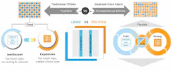
As the next generations of FPGA devices with highly efficient architectures are introduced to the market, they raise a very interesting dynamic to the traditional technology tradeoffs available to designers. Since their functionality is completely in the hands of the designer, they can be configured to expose the parallelism of a GPU, the software programmability of a CPU, and the domain specific efficiency of custom silicon.
The extent to which tradeoffs favor each of these characteristics can be changed dynamically. This allows a flexible design philosophy in which an early version of an application might favor a fast time-to-market software approach while later revision might seek to improve performance by increasing parallelism. At the same time, system performance and the overall bill of materials can be optimized by embracing concepts borrowed from custom silicon.
The possibility of taking a heterogeneous approach to system design enables designers to select the appropriate technology for each portion of the solution:
- A pure software approach running in an embedded processor for areas of control code, interfaces, or communications stacks.
- A hardware-accelerated software portion for pre- or post-processing of data or for areas requiring lower performance AI algorithms.
- A pure, massively parallel approach for high-performance AI models.
- A dedicated hardware approach for signal processing and signal conditioning.
All of these techniques can be used interchangeably in the same edge application and in a highly efficient, low-power, and cost-effective hardware footprint.
They might evolve as the design matures and the lines dividing them might start to blur. A software algorithm running on an embedded processor might be progressively accelerated by designing hardware accelerators in the FPGA fabric. These accelerators can be used to replace large sections of software delivering hardware speed under software control. Progressively more accelerators can be instantiated in the FPGA fabric to achieve required performance levels.
The reprogrammable nature of the FPGA lends itself naturally to this iterative and progressive approach to system design, as a system expressed as a software algorithm is migrated to take full advantage of the parallel hardware instantiated in the FPGA.
Of note in this design philosophy is the advent of the RISC-V processor. The RISC-V instruction set architecture is open source and many implementations are freely available. These processor implementations are available as intellectual-property blocks and can be instantiated inside the configurable fabric of the FPGA. The FPGA fabric then takes on the role of the embedded processor and is available to run code to implement the software portion of this hybrid development flow.
Not all instructions in the RISC-V instruction set architecture are defined, though. Many are left open for the user to define and can serve to direct execution to hardware accelerators within the FPGA fabric. Software running on the RISC-V processor can call a custom instruction and have the instruction complete in a fully custom ALU running on the FPGA fabric before control is handed back to the next software instruction. Progressive acceleration of software functionality using hardware accelerators is therefore rapid and intuitive.
Conclusion
The desire to exploit the unique advantages of AI at the far edge of the network is creating extremely challenging requirements and design constraints. None of the traditional design approaches are optimal to meet these requirements except for the latest families of ultra-efficient FPGAs.
Such FPGAs bring design flexibility, time-to-market advantages, and parallel compute capabilities at hardware speed in a low-power, small physical footprint. Their ability to absorb additional system functionality within their programmable fabric further reduces system cost.
A heterogeneous design philosophy reduces time-to-market, while an iterative design philosophy reduces program risk. These ultra-efficient FPGAs facilitate edge designs by providing a versatile and flexible compute capability for the integration of AI at the network’s edge.
>>Download the PDF of this article, and check out the TechXchange for similarly themed content

 Edge AI TechXchange
About the Author
 Mark Oliver
Mark Oliver
VP of Marketing and Business Development, Efinix Inc.
Mark Oliver is an industry veteran with extensive experience in engineering, applications, and marketing. A native of the UK, Mark gained a degree in Electrical and Electronic Engineering from the University of Leeds. During a 10-year tenure with Hewlett Packard, he managed Engineering and Manufacturing functions in HP Divisions both in Europe and the U.S. before heading up Product Marketing and Applications Engineering at a series of video related startups.
Prior to joining Efinix, Mark was Director of Worldwide Storage Accounts at Marvell, leading the Marketing and Business Development activities.
Comment About the Article
To join the conversation, and become an exclusive member of Electronic Design, create an account today!
 Leaders Logo
Leaders relevant to this article: