Why AI-Driven Chip Design Requires Physics-Aware Co-Optimization
What you’ll learn:
- How agentic AI has moved beyond copilots to coordinate multi-step design and verification workflows.
- Why engineers remain responsible for specifications, tradeoffs, and validation.

AI has changed what’s possible in semiconductor engineering, evolving from a simple copilot to performing complex chip design tasks.
The rise of physical AI and the growing demand for custom silicon have created a greater need for chips designed specifically for AI workloads. Today, there’s a growing gap between the fast pace of AI model development and traditional chip-development timelines. As models and workloads change every few months, semiconductor teams face rising pressure to shorten time-to-market.
These technical and business pressures are beginning to exceed what humans alone can handle. Engineering teams are being asked to take on more projects; shorten design cycles; improve power, performance, and area (PPA); and keep compute and engineering costs in check. Simply put, teams need to manage more variables in less time.
That’s changing how AI factors into chip development. Previously, AI in chip design has primarily taken the form of copilots, code assistants, or point solutions that help engineers with individual tasks. Agentic AI goes one step further by coordinating multi-step workflows and working toward defined design and verification outcomes.
For instance, AI agents can take a verification goal, identify the steps needed to get there, run the necessary tools, learn from the results, and continue working until the design fulfills the target. All of this happens in a timescale that would be difficult for humans to match.
Why General-Purpose Agents Fall Short in Chip Design
What’s driving the shift toward domain-specific multi-agent systems handling different parts of the engineering process?
For starters, general-purpose large language model (LLM) agents can help with certain tasks, but production chip design requires in-depth domain knowledge, tighter integration with engineering tools, and the capability to manage complex workflows. In particular, generic agents struggle with:
- Long-horizon tasks: Lengthy tool runs and interconnected steps make it difficult for generic agents to preserve context and manage a task from start to finish.
- AI errors: Mistakes in reasoning, RTL changes, or how the results are interpreted can compound as work moves from one step to the next.
- Compute inefficiency: Processing large reports repeatedly or retrying failed steps can waste compute resources without producing the intended result. With so many factors to consider, teams can’t simply connect an LLM to design tools and expect production-ready results. They need a purpose-built system for semiconductor engineering that combines the domain expertise, specialized workflows, tools, and models needed to handle chip design complexity.
How Agents Generate, Refine, and Verify Outcomes
What really differentiates agentic AI is its ability to move beyond helping with an individual task and work through a complex engineering problem from start to finish.
A typical agentic workflow may start with a design requirement. The agents will determine what steps need to be done and generate or update the RTL as needed. From there, they will run the appropriate engineering tools, review the results, and check for failures or opportunities to improve PPA. Based on the findings, agents can make adjustments, rerun the tools, and repeat the process until the design satisfies its target.
Root cause analysis is a strong example of this process. One such example is ChipAgent’s autonomous root cause analysis (RCA) flow. Agents trace simulation failures to their root causes by combining RTL, testbench, log, and waveform analysis. Its waveform engine lets agents query specific signal events without loading entire waveform databases into context. Parallel prover–verifier pairs propose and check root-cause hypotheses against code and waveform evidence, while a self-consistency layer ranks their conclusions by confidence. Engineers receive ranked explanations, supporting traces, and bug resolutions for review.
This approach is already being applied in production. At Whalechip, agentic AI helped engineers identify four critical bugs in a memory controller, including a hidden three-cycle race condition. By automating analysis across complex design data, the team reduced RCA from days to as little as 15 minutes.
This feedback-driven process allows AI agents to work independently. Instead of helping with just one step, agents work across the full loop, from understanding the goal to executing, evaluating results, making corrections, and verifying the outcome. In a multi-agent system, specialized agents can take on different parts of the workflow and collaborate toward the same engineering objective.
Bringing Physics Intelligence Early into RTL Decisions
One of the biggest challenges in chip design is that early RTL decisions can significantly affect timing and power, but engineers don’t see those effects until much later in the process. This can lead to considerable rework downstream as well as longer design cycles (see figure).
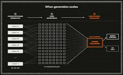
A physics-aware surrogate model can offer a way to move up that feedback by serving as a faster stand-in for later design tools. By learning from previous RTL designs and their downstream results, these models can predict the most likely timing and power outcomes much earlier, helping engineers spot problems before they prove costly.
This is important for agentic AI designs. Autonomous agents need fast, reliable feedback about how design changes will affect the chip’s physical performance. Without that insight, they may have to run costly and slow simulations repeatedly to determine whether each change is moving the overall design process in the right direction. Getting that PPA feedback earlier can drastically reduce unnecessary design iterations, lower compute and software costs, and shorten development time.
Making AI Models and Engineering Tools Work Together Securely
No single AI model or agent can handle every aspect of chip design. Making agentic AI effective in semiconductor development requires a full-stack approach in which models, workflows, and engineering tools work together. It must also account for physics-aware feedback and protect sensitive design data. This depends on three key elements:
- Models: Reasoning and planning models work alongside specialized, physics-aware models to help optimize multiple design projectives.
- Workflows: Agentic workflows that carry persistent design intent and manage long-running, multi-step design processes.
- AI-native tools: Tools enable agents to perform actions faster, interpret results more accurately, and get earlier feedback to determine ensuing steps. Together, these layers allow the AI to understand the design, anticipate how changes will affect physical performance, pick the right tools and workflows, and keep improving the design until it reaches the desired engineering result. Just as important is the ability to preserve and build on an organization’s design knowledge, so that agents can learn from past engineering decisions and improve over time.
Security is also essential to consider in semiconductor design. On-premises deployment and training can help keep sensitive design data, proprietary methods, and institutional knowledge behind a customer’s firewall.
A New Role for Semiconductor Engineers
Even as agentic AI takes on more of the execution, engineers remain responsible for defining semiconductor specifications, constraints, architectural priorities, PPA tradeoffs, and final validation.
What changes is how much of the work between those decisions they need to handle themselves. Agents can take on more of the repetitive, iterative execution, allowing engineers to spend more time using their expertise and judgment. Their role becomes one of guiding the overall process, evaluating results, and stepping in for exceptions or critical design decisions.
This change can have a critical impact on engineering teams, helping them explore more alternatives, accomplish more design work, and shorten the path from specification to verified design.
A Faster Path from Specification to Verified GDS
As these capabilities mature, agentic AI can change how semiconductor teams move from an initial design goal to a verified outcome.
The larger shift in chip development is from engineers operating tools step by step to working toward broader engineering objectives. Engineers define what needs to be built, whereas autonomous systems handle how the work is carried out, evaluated, refined, and verified.
The result is a faster, more iterative design process that gives engineers more time to focus on architecture, tradeoffs, and the decisions that require their expertise.
>>Download the PDF of this article
 id_346942363__nicoelnino__dreamstime
About the Author
 Solaiman Rahim
Chief Product Officer, ChipAgents
Solaiman Rahim is Chief Product Officer at ChipAgents, where he leads product strategy and development for the company’s agentic AI platform for semiconductor design and verification. He has more than 25 years of experience in chip automation, AI, and semiconductor design. Previously, he served as Vice President of R&D at Synopsys and held senior leadership roles at Atrenta.
Rahim holds a Ph.D. in formal verification and has more than 20 patents spanning AI, formal verification, synthesis, power, timing, and ECO.
Related
id_346942363__nicoelnino__dreamstime ai_dreamstime_jaroonittiwannapong_353844208


Comment About the Article
To join the conversation, and become an exclusive member of Electronic Design, create an account today!
 Leaders Logo
Leaders relevant to this article: